August 25, 2004... Device Offers Radiant Power Up to 180 mW/sr for Higher Performance, Cost Savings in Consumer, Industrial Products
PALO ALTO, California USA -- Agilent Technologies Inc. (NYSE: A) today introduced a new high-speed LED infrared (IR) emitter. The new product, from Agilents Semiconductor Products Group, uses the companys high-power aluminum gallium arsenide ( AlGaAs) LED technology, which has been optimized for high radiant intensity, speed and low forward voltage.
The Agilent HSDL-4261 IR emitter provides manufacturers with a low-cost illumination source suitable for a broad range of applications, from communication devices and IR LANs to consumer products such as optical mice, IR headphones, microphones and keyboards.
The HSDL-4261 emitter features 15 ns rise time and 45 ns fall time (10 percent to 90 percent), with intensities of up to 180 mW/sr (typical) at ILED=100 mA at a 26-degree viewing angle. It operates At the 870 nm optical wavelength and is supplied in an industry-standard 5 mm (T-1 3/4) form-factor package.
The Agilent IR emitter is built with iron lead frames that dissipate power during over a wide range of currents. The forward voltage is a low 1.40 volts at 20 mA, which, in some applications, allows two or more of the emitters to be connected in Series without exceeding the supply-voltage capability.
US Pricing and Availability
The Agilent HSDL-4261 is priced at $0.12 each in moderate volumes and is available now through Agilents direct sales channel and worldwide distribution partners.
Further information about Agilents infrared products is available at
About Agilent Technologies
Agilent Technologies Inc. (NYSE: A) is a global technology leader in communications, electronics, life sciences and chemical analysis. The companys 28,000 employees serve customers in more than 110 countries. Agilent had net revenue of $6.1 billion in fiscal year 2003. Information About Agilent is available on the Web at

HDI Pcb
Hdi Pcb Specification
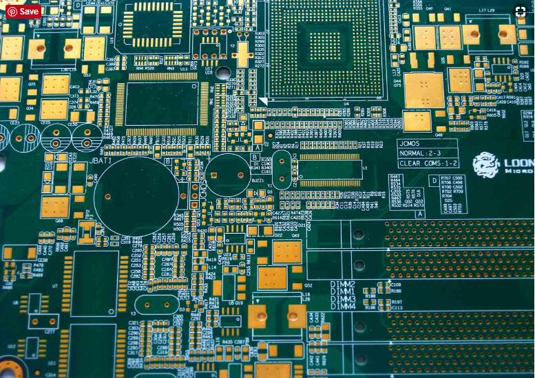
High density interconnect (HDI) PCBs represent one of the fastest-growing segments of the printed circuit board market. Because of its higher circuitry density, the HDI PCB design is able to incorporate finer lines and spaces, smaller vias and capture pads, and higher connection pad densities. A high density PCB features blind and buried vias and often contains microvias that are .006 in diameter or even less.
Key HDI PCB Benefits
The evolution of high density PCB technology has given engineers greater design freedom and flexibility than ever before. Designers now have the ability to place more components on both sides of the raw PCB if desired. In essence, an HDI PCB gives designers more space to work with, while allowing them to place smaller components even closer together. This ultimately results in faster signal transmission along with enhanced signal quality.
HDI PCB is widely used to reduce the weight and overall dimensions of products, as well as enhancing the electrical performance of the device. It's regularly found in mobile phones, touch-screen devices, laptop computers, digital cameras, 4G network communications, also prominently featured in medical devices as well as various electronic aircraft parts and components.

Over the course of a decade in business, Topscom has established a hard-earned reputation for manufacturing PCBs of the highest quality. Our custom PCB manufacturing capabilities enable you to get the finest quality HDI PCBs at competitive prices without min order quantity requirement. Our team run design for manufacture check on your custom PCB file and consult with you to ensure it is ready for manufacturing and that your boards will meet your performance requirements. We also have an on-site quality control department to verify the finished product meet your high quality standards.
|
HDI Structures |
Type of Micro vias |
Mass Production |
Small-Middle Batch |
Prototype | Available |
| 1+N+1 | Blind vias | Yes | Yes | Yes | 4 layers+ |
| 2+N+2 |
Blind/Buried staggered vias |
Yes | Yes | Yes | 6 layers+ |
| 2+N+2 |
Blind/Buried stacked vias |
Yes | Yes | Yes | 6 layers+ |
| 3+N+3 |
Blind/Buried staggered vias |
/ | Yes | Yes | 8 layers+ |
| 3+N+3 |
Blind/Buried stacked vias |
/ | / | Yes | 8 layers+ |
Check our HDI PCB capabilities by reviewing the table found below:
| Feature | Capability |
| Quality Grade | Standard IPC 2 |
| Number of Layers | 4 - 24layers |
| Order Quantity | 1pc - 10000+pcs |
| Build Time | 2days - 5weeks |
| Material | FR4 standard Tg 140°C,FR4 High Tg 170°C, FR4 and Rogers combined lamination |
| Board Size | Min 6*6mm | Max 457*610mm |
| Board Thickness | 0.4mm - 3.0mm |
| Copper Weight (Finished) | 0.5oz - 2.0oz |
| Min Tracing/Spacing | 2.5mil/2.5mil |
| Solder Mask Sides | As per the file |
| Solder Mask Color | Green, White, Blue, Black, Red, Yellow |
| Silkscreen Sides | As per the file |
| Silkscreen Color | White, Black, Yellow |
| Surface Finish |
HASL - Hot Air Solder Leveling Lead Free HASL - RoHS ENIG - Electroless Nickle/Immersion Gold - RoHS Immersion Silver - RoHS Immersion Tin - RoHS OSP - Organic Solderability Preservatives - RoHS |
| Min Annular Ring | 4mil, 3mil - laser drill |
| Min Drilling Hole Diameter | 6mil, 4mil - laser drill |
| Max Exponents of Blind/Buried Vias | stacked vias for 3 layers interconnected, staggered vias for 4 layers interconnected |
| Other Techniques |
Flex-rigid combination Via In Pad Buried Capacitor (only for Prototype PCB total area ≤1m²) |
HDI Pcb
Hdi Pcb,Hdi Pcb Boards,Hdi Pcb Printed Circuit Boards
Topscom Technology Co., Ltd. , http://www.pcbassemblycn.com