Serial peripheral interface (SPI) is a synchronous serial interface from Motorola that allows CPU and TTL shift registers, A/D or D/A converters, real-time clock (RTO), The memory and peripheral interface devices such as LCD and LED display drivers communicate in a serial manner.
The SPI bus requires only 3 to 4 data lines and control lines to expand various I/O devices with SPI interfaces. The hardware functions are very strong and the software is quite simple. The serial A/D converter has the characteristics of simple circuit and reliable operation, and the ARM chip is designed for the integrated system of handheld devices and common embedded applications, combining the above two practical chips and SPI bus technology. Data collection is very effective.
1 AD7888 features and use
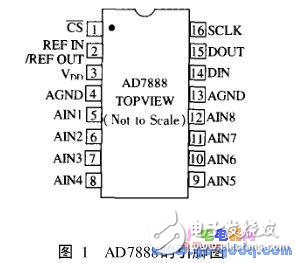
The AD7888 is a high-speed, low-power, 12-bit A/D converter from Analog Devices, Inc. that operates from a single 2.7 to 5.25 V supply and has a maximum throughput of 125 kSPS. The AD7888's input sample/hold circuit acquires a signal in 500 ns in single-ended sampling mode with eight single-ended analog inputs with analog input voltages from 0 to VREF. The AD7888 has an on-chip 2.5 V reference and can also use an external reference from 1.2 V to VDD. The CMOS manufacturing process ensures low power consumption of 2 mW during normal operation and 3uW in power-down state. Multiple power management modes (including automatic power-down mode after data conversion) are available, compatible with a variety of serial interfaces (SPI/QSPI/MICOWIRE / DSP). The AD7888 can be used in a wide range of battery-powered systems (personal digital assistants, medical instruments, mobile communications), instrumentation control systems, and high-speed modems. The device is available in 16-pin SOIC and TSSOP outline packages. The outline and pin definitions are shown in Figure 1 and Table 1.
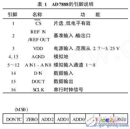
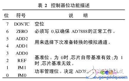
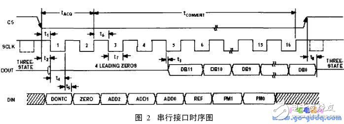
Figure 2 shows a detailed serial interface timing diagram that provides conversion timing and controls the input and output of the AD7888 conversion information. The CS initializes data transfer and conversion processing. The input signal is sampled at 1.5 clock cycles after its falling edge, which is expressed as tACQ (acquisition time). The entire conversion process also takes 14.5 clock cycles to complete, which is expressed as tCONVERT (conversion time).
The entire conversion process to get data from the AD7888 takes 16 clock cycles. After the rising edge of CS, the bus returns to a high-impedance state. If CS continues to be low, prepare for a new round of conversion. The selection of the input channel for sampling is written to the control register in advance, so when converting, the user must write in advance to prepare for the conversion of the channel. That is to say, when the current conversion is performed, the user must write the address of the channel in advance for the next conversion.
The main functions of the 2S3C2410
The S3C2410 is a 16/32-bit microprocessor from Samsung that uses a RISC architecture. It is based on the ARM920T core and features a five-stage pipeline and a Harvard architecture with a maximum frequency of 203 MHz. It is a hard macrocell with high performance and low power consumption. The ARM920T features an ARM-enhanced MMU (supports WinCE, EPOC 32 and Linux), 16kB of instruction and data cache, and a high-speed AMBA bus interface.
The S3C2410 is designed for use in handheld devices and integrated systems for embedded applications. To reduce overall system cost, the S3C2410 includes the following sections: LCD Controller (STN&TFT), NAND Flash Boot Loader, System Management (Chip Select) Logic and SDRAM controller), 3-channel UART, 4-channel DMA, 4-channel PWM clock, I/O port, RTC, 8-channel 10-bit ADC and touch screen interface, IIC bus interface, IIS bus interface, USB host port and USB device Port, SD main port and multimedia card interface, 2-channel SPI and 2-channel PLL.
The S3C2410 has two SPI ports for serial data transmission. Each SPI interface has two shift registers for receiving and transmitting data. During data transmission, the transmission data and the reception data are synchronized, and the frequency of transmission can be set by the corresponding control register. If you only want to send data, the received data is a dummy; if you only want to receive the data. Then you need to send the dummy "0xff". The SPI interface has four pin signals: serial clock SCK (SPICLK0, 1), master-in slave-out MISO (SPICLK0, 1), and master-slave-in-in-MOSI (SPIMOSI0, 1) data lines, active-low pin/ SS(nSSO, 1).
The S3C2410's SPI interface has the following features:
(1) Compatible with SPI protocol (ver.2.11);
(2) There are 8-bit shift registers for transmission and reception, respectively;
(3) There is an 8-bit register that sets the transmission frequency;
(4) There are three transmission modes: polling, interrupt and DMA.
3 interface and drive
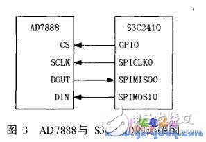
According to the SPI characteristics of the S3C2410 and the working principle of the AD7888, the interface is determined as shown in Figure 3.
The control register of the AD7888 is an 8-bit write-only register. Data is loaded from the DIN pin on the rising edge of SCLK while the result of the external analog conversion is taken. Each successive data transfer requires preparation of 16 consecutive clock signals. Only the information provided on the rising edge of the first 8 clock pulses after the chip select signal falls is loaded into the control register.
In order to realize the high-speed A/D conversion of S3C2410 and AD7888 under embedded Linux, a driver for both interfaces is also written. The implementation of the driver function is mainly accomplished by the following functions.
(1) Init_SPI () completes the initialization of the SPI
Void Init_SPI(void)
{
Int i;
rSPPRE0=0x32;
rSPCON0=0x1e;
For(i=0;iCS
rGPHCON |=0x0400;
rGPHCON&=(~0x0800);
rGPHUP&=(~0x20);
rGPHDAT |=0x20;
}
(2) ad_wr() writes the channel that requires A/D conversion
staTIC ssize_t ad_wr(struCt file *file,const char *bur,size_t count,loft_t *offset)
{
Int ret=“0â€;
Int i=“0â€;
Dbuf=“kmalLOC†(count *sizeof(unsigned char), GFP_KERNEL);
Copy_from_user(dbuf,bur,count);
For(i=0;i ADTXdata[i]=dbuf[i];
Kfree(dbuf);
Return ret;
}
(3) ad_rd () get the result of A / D conversion
staTIe ssize_t ad_rd(struet file *file,char *bur,size_t count,loft t *offset)
{
Int ret=“0â€;
Int i=“0â€;
Ad_convert();
Ad_convert();
Dbuf=“kmallocâ€(count *sizeof(unsigned char), GFP KERNEL);
For(i=0;i dbuf[i]=ADRXdata[i];
Copy_to_user(bur,dbuf,count);
Kfree(dbuf);
Return ret;
}
(4) ad_convert() actually completes the A/D conversion
Void ad_convert(void)
{
rGPHDAT&=(~0x20);
Udelay (100000);
Spi_tx_data(ADTXdata[0]);
ADRXdata[0]=rSPRDATO;
Spi_tx_data(0xff);
ADRXdata [1 ]=rSPRDATO;
rGPHDAT |=0x20;
}
(5) spi_tx_data() completes sending data
Void spi_tx_data(unsigned char data)
{
Spi_poll_done();
rSPTDAT0=data;
Spi_poll_done();
}
(6) spi_poll_done() polls SPI status
StaTIC void spi_poll_done(void)
{
While(!(rSPSTA0&0x01));
}
Laptop power adapter charger for Macbook, Macbook Air and Macbook Pro.
45w, 60w, 80w charger with Magsafe 1 or Magsafe 2 connector.
Four replacement ac plugs for your choices, US / EU / UK / AU plug as your requirement.
Stable output and high charging efficiency.
Elegant outlook design as original one, touch smoothly and comfortable.
Easy carry if you want to take your computer outside for business or travel.
Original charger is good, but as a replacement, our product has more reasonable price when your original charger is broken.
And, the market of the replacement adapters becomes bigger and bigger. People would rather buy a copy one then the original because of the price.
But at the same time, people worry about that they will buy something defective. So the problem comes, how to buy a good quality one with a good price?
As a professional power adapter manufacturer, we have excellent R&D team, skilled staffs and responsible after-sale service. All your benefits can be under protected after you buy products for our company.
Our certificates :ISO9001:2008 & ISO14001:2004 , CCC , CE , FCC , ROHS.
All our products has 1 year warranty. In other words, if you get the dad products which are not damaged physically from us in one year, we will replace you the new one or the whole bulk order.
Macbook Adapter,45W Adapter For Macbook,45W Charger For Macbook,60W Charger For Macbook,Macbook Charger
Shenzhen Waweis Technology Co., Ltd. , https://www.huaweishiadapter.com