We often compare the crystal oscillator to the heart of the digital circuit. This is because all the work of the digital circuit is inseparable from the clock signal. The crystal oscillator directly controls the whole system. If the crystal oscillator does not work, the whole system will be paralyzed, so the crystal oscillator is decided. A prerequisite for the digital circuit to start working.
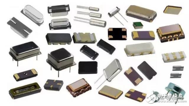
The crystal oscillators we often say are quartz crystal oscillators and quartz crystal resonators. They are all made by the piezoelectric effect of quartz crystals. Applying an electric field to the two electrodes of the quartz crystal causes mechanical deformation of the crystal. Conversely, if mechanical pressure is applied to both sides of the crystal, an electric field is generated on the crystal. And, these two phenomena are reversible. With this characteristic, an alternating voltage is applied to both sides of the crystal, and the wafer generates mechanical vibration while generating an alternating electric field. This type of vibration and electric field is generally small, but at a certain frequency, the amplitude is significantly increased. This is the piezoelectric resonance, similar to the LC loop resonance we often see. 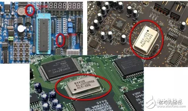
As the heart of digital circuits, how does crystal oscillator work in smart products? For smart homes such as air conditioners, curtains, security, surveillance and other products, wireless transmission modules are required. They send modules from one end to the other through Bluetooth, WIFI or ZIGBEE protocols, or directly through the mobile phone, and the crystal oscillator is The core components in the wireless module affect the stability of the whole system, so choosing the crystal oscillator used by the system determines the success or failure of the digital circuit.
Due to the importance of the crystal oscillator in digital circuits, we need to be careful when using and designing:
1. There is a quartz crystal inside the crystal oscillator. When the external impact or drop occurs, the quartz crystal breaks and breaks, and the crystal oscillator does not vibrate. Therefore, when designing the circuit, consider the reliable installation of the crystal oscillator. The position should be as close as possible to the edge of the board and the device casing. Wait.
2. Pay attention to the welding temperature when welding by hand or machine. The crystal is sensitive to temperature, the temperature during soldering should not be too high, and the heating time should be as short as possible.
Reasonable crystal layout can suppress system radiation interferenceFirst, the problem description
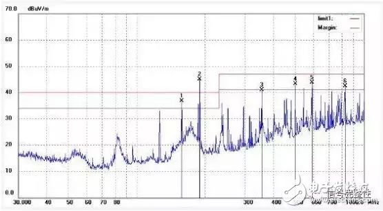
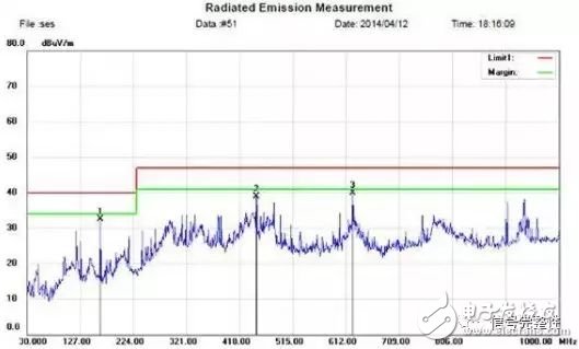
The product is a field camera, which is divided into five parts: the core control board, the sensor board, the camera, the SD memory card and the battery. The outer casing is a plastic case. The small board has only two interfaces: DC5V external power interface and USB interface for data transmission. Radiation tests have found that there are about 33MHz harmonic noise problems.
The original test data is as follows:
Second, analyze the problem
The outer casing of the product is a plastic casing. It is a non-shielded material. The whole machine only tests the power cable and the USB cable to pull out the casing. Is the interference frequency radiated by the power cable and the USB cable? Therefore, I made a few steps to test:
(1) Add a magnetic ring only on the power line, the test result: the improvement is not obvious;
(2) Adding a magnetic ring only on the USB cable, the test result: the improvement is still not obvious;
(3) Add magnetic rings to both the USB cable and the power cable. The test results are: the improvement is obvious, and the interference frequency is reduced overall.
From the above, the interference frequency is brought out from the two interfaces. It is not a problem of the power interface or the USB interface, but the internal interference frequency is coupled to the two interfaces. Only shielding one interface cannot solve the problem. problem.
After near-field measurement, the interference frequency comes from a 32.768KHz crystal oscillator on the core control board, which generates strong spatial radiation, so that the surrounding trace and GND are coupled with 32.768KHz harmonic noise, and then through the interface. The USB cable and the power cable are coupled out to radiate. The problem with this crystal is caused by the following two problems:
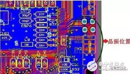
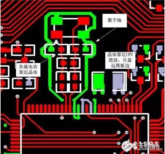
(1) The crystal oscillator is too close to the edge of the board, which is likely to cause crystal radiation noise.
(2) There is a cloth signal line under the crystal oscillator, which is easy to cause harmonic noise of the signal line to couple the crystal oscillator.
(3) The filter component is placed under the crystal oscillator, and the filter capacitor and the matching resistor are not arranged according to the signal flow direction, so that the filter effect of the filter component is deteriorated.
Third, the solution
According to the analysis, the following countermeasures are obtained:
(1) The filter capacitor and matching resistor of the crystal are placed close to the CPU chip, away from the edge of the board;
(2) Remember that the floor cannot be placed in the crystal placement area and the lower projection area;
(3) The filter capacitor and matching resistor of the crystal are arranged according to the flow direction of the signal, and are placed neatly and compactly close to the crystal;
(4) The crystal is placed close to the chip, and the trace between the two is as short and straight as possible.
Can refer to the following layout:
After the rectification, the prototype test results are as follows:
Fourth, the conclusion
Many system crystal oscillators today have many system crystal clocks with high clock frequency and strong interference harmonic energy. Interfering harmonics are radiated from space except for the two traces of their input and output. If the layout is unreasonable, it is easy to cause strong The problem of noise radiation is difficult to solve by other methods, so it is very important to layout the crystal and CLK signal lines during PCB layout.
Crystal PCB PCB Design Considerations(1) The coupling capacitor should be placed as close as possible to the power supply pin of the crystal oscillator. The position is placed in the order of the power supply inflow direction. The capacitance values ​​are placed from the largest to the smallest, and the capacitor with the smallest capacitance is closest to the power supply pin.
(2) The outer shell of the crystal must be grounded, radiated outward from the crystal, or shielded from external signals to interfere with the crystal.
(3) Do not route the crystal under the crystal to ensure complete grounding, and do not route the crystal within 300 mil range. This will prevent the crystal from interfering with the performance of other wiring, devices and layers.
(4) The trace of the clock signal should be as short as possible, the line width should be larger, and the balance should be found in the length of the wiring and away from the heat source.
(5) Do not place the crystal on the edge of the PCB. Pay special attention to this point when designing the board.
Focusing on the development and production of Wireless Charging products that make life easier.
Supply various wireless charger including multifunctional Wireless Charger, Car Wireless Charger, Magnetic Wireless Chargin, Wireless Charging Mouse Pad, etc.
We help 200+ customers create custom wireless charging products design for various industries.
Manufacturing high quality products for customers according to international standards, such as CE ROHS FCC REACH UL SGS BQB etc.
Wireless Charging Pad,Wireless Phone Charger,Wireless Car Charger,Bluetooth Charger
TOPNOTCH INTERNATIONAL GROUP LIMITED , https://www.micbluetooth.com