When the main power supply is cut off, the circuit automatically cuts in the battery through the relay to supply power to the device. When the main power supply is normal, the battery is charged in different modes: when the voltage is greater than the set value, the constant voltage is charged; when the voltage is lower than the set value, the constant current is charged. Test results prove that the system can protect the circuit from overcurrent and undervoltage through relays.
0 Preface
The indicator requirements for this design:
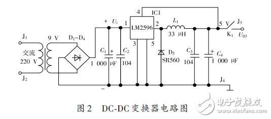
The battery is 4.2 V and the load is 5 V. For this purpose, the switching voltage regulator LM2596 is used for DC-DC conversion, which has the characteristics of strong driving capability and good linearity. The main features of the uninterruptible DC power supply are as follows: When the main power supply is normal, in addition to supplying power to the equipment, the battery can be charged in different modes. When the voltage is greater than 4.2 V, the constant current charging circuit is cut off, and the constant voltage charging circuit is turned on. When the voltage is lower than 4.2 V, the constant current charging is maintained; the constant voltage charging is composed of W117 and the operational amplifier LM324, and has the characteristics of stable output and small ripple. Constant current charging consists of high-power field tube IRF640 and op amp LM324. It has the characteristics of high output current precision, small ripple, and small output current affected by load. If the main power supply is cut off, the battery will be cut automatically to keep the power supply uninterrupted. .
1 system design
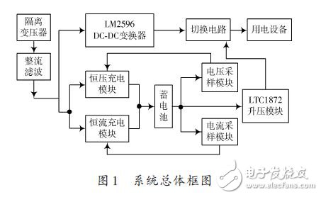
1.1 System overall block diagram
According to the system design requirements, the uninterruptible DC power supply has: uninterrupted power supply to the device when there is no AC power; when the AC power is normal, there are two modes of constant voltage charging and constant current charging; comprehensive design requirements, forming a system block diagram as shown in the figure 1 is shown.
1.2 Selection of DC-DC converter scheme
Using the switching voltage regulator LM2596, it can output 3 A of driving current, and has good linearity and load regulation characteristics. It can fix output voltages of 3.3 V, 5 V, and 12 V, and can also achieve 1.2 to 37 V. Adjustable output between.
The device integrates a frequency compensation and fixed frequency generator with a switching frequency of 150 kHz, which allows the use of smaller filter components compared to low frequency switching regulators. Since the device requires only four external components, a common standard inductor can be used, which simplifies the use of the LM2596 and greatly simplifies the design of the switching power supply circuit. Under the conditions of specific input voltage and output load, the error of the output voltage can be guaranteed within ±4%, and the oscillation frequency error is within ±15%. External power-down can be achieved with a standby current of only 80 μA; it has a self-protection circuit (a two-stage down-conversion current limit protection and an over-temperature full protection circuit that is powered down in an abnormal situation).
The DC-DC converter circuit is shown in Figure 2.
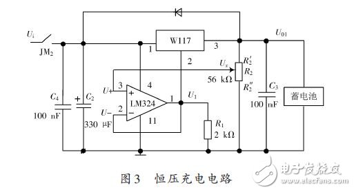
1.3 Constant voltage charging circuit design
The constant voltage charging circuit is shown in Figure 3. The circuit consists of an op amp LM324 and a three-terminal regulator W117. The LM324 is connected as a voltage follower with an output voltage U1 = U- = U+ = UX. It can be seen that the output voltage can be changed by adjusting the middle tap of resistor R2. Due to the presence of the op amp, the output voltage is adjusted very smoothly.
1.4 Voltage Control Constant Current Charging Circuit Design
The circuit principle is shown in Figure 4. The constant current source circuit is composed of an operational amplifier LM324, a field effect transistor IRF640, a sampling resistor R3, a load resistor RL, and the like.
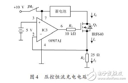
The circuit uses a high-power FET IRF640 as an adjustment tube. The tube is an N-channel enhancement MOS transistor. The tube operates up to 100 V, has a saturated drain current of 28 A, and consumes about 150 W. When the effect transistor is operating in the saturation region, the drain current Id is approximately the current controlled by the voltage Ugs. That is, when Ud is a constant, it satisfies: Id = f (Ugs), and as long as Ugs is unchanged, Id does not change.
In this circuit, R2 is the sampling resistance of the constantan wire material (the resistance changes little with temperature). OP07 acts as a voltage follower with U+ = U - = Us. Since the gate current is negligible, Id = Is = I2 = Us R2 = U+ R2. Just because Id = U+ R2, the circuit input voltage U+ controls the current Id. That is, Id does not change with the change of RL, thereby achieving voltage-controlled constant current. The parameter charging current in Figure 4 is 200 mA. To change the charging current, simply adjust R2.
Single Phase Voltmeter,Led Single Phase Voltmeter,Voltage Measurement Tool,Digital Voltmeter
zhejiangjinyidianqiyouxiangongsi , https://www.jooeei.com