
After the chicken screamed, the sun had not yet fully risen above the horizon. The air was still cool and quiet, and the old store welcomed its first customer of the day.
The shopkeeper greeted, “It’s really early here—what brings you by so soon?â€
“I’m looking for input devices for a SAR ADC analog input architecture.â€
“Well, do you want a single-ended input, a pseudo-differential input, or a differential input?â€
The customer frowned slightly, “Why are there so many options?â€
The shopkeeper smiled and said, “These input types are all available. Let’s start with the basics…â€

What is a SAR ADC?
Successive Approximation Register Analog-to-Digital Converters, or SAR ADCs, are general-purpose ADCs that convert continuous analog signals into discrete digital representations. They work through a charge redistribution process where a known amount of charge is compared to the charge at the ADC input. During this process, a binary search is performed across all possible digital codes (quantization levels), and the final result converges to a specific code. This causes the internal comparator to return to equilibrium. The combination of 0s and 1s represents the decision sequence generated by the circuit, bringing the system back to balance.
SAR ADCs are versatile, low-power, and easy to use. However, when choosing one for a specific application, there are several options to consider. This article focuses on the types of analog inputs offered in the ADI SAR ADC portfolio. While the discussion centers on SAR ADCs, these input types are common across all ADC architectures. Depending on the signal source or the overall design goals, certain trade-offs must be made. The simplest approach is to match the ADC input type to the source output configuration. But sometimes, the signal may need conditioning, or cost, power, or area considerations might influence the choice. Let's explore the different analog input types available.
Single-Ended Input
The simplest analog input type is the single-ended input. In this case, the signal only needs one wire from the source to the ADC. A single input pin is used, and there is no direct return path or sensing loop. The conversion result is measured relative to the ADC’s ground pin. Depending on the device, the input can be unipolar or bipolar. Single-ended configurations are simple and reduce system complexity, which also lowers power consumption in the signal chain. However, they don’t suppress DC offsets, and voltage differences between the source ground and the ADC ground can affect the conversion results. Additionally, they are more susceptible to noise coupling, so the signal source and ADC should be placed close together to minimize interference.
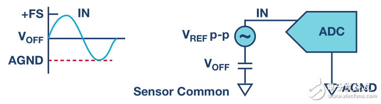
Figure 1. Single-Ended Unipolar
If the SAR ADC is in a unipolar single-ended configuration, the signal swing ranges from ground to the positive full scale, typically set by the ADC reference. A visual example of a single-ended unipolar input is shown in Figure 1. Devices like the AD7091R and AD7091R-8 feature this type of input.
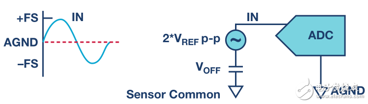
Figure 2. Single-Ended Bipolar
In a bipolar single-ended configuration, the signal swing ranges from negative full scale to positive full scale. Again, the full-scale range is usually determined by the ADC reference. The figure above illustrates a single-ended bipolar input. An example of such a device is the AD7656A-1.
Pseudo-Differential Input
When a signal requires measurement relative to a ground point rather than the current-carrying path, a pseudo-differential input structure may be considered. A pseudo-differential ADC functions as a single-ended device but references its ground. It performs a differential measurement, but the sensed differential voltage is based on the single-ended input relative to the input signal ground. The single-ended input is connected to the positive ADC input (IN+), while the signal ground is connected to the negative input (IN–). Designers must pay attention to the allowable input range of the negative pin.
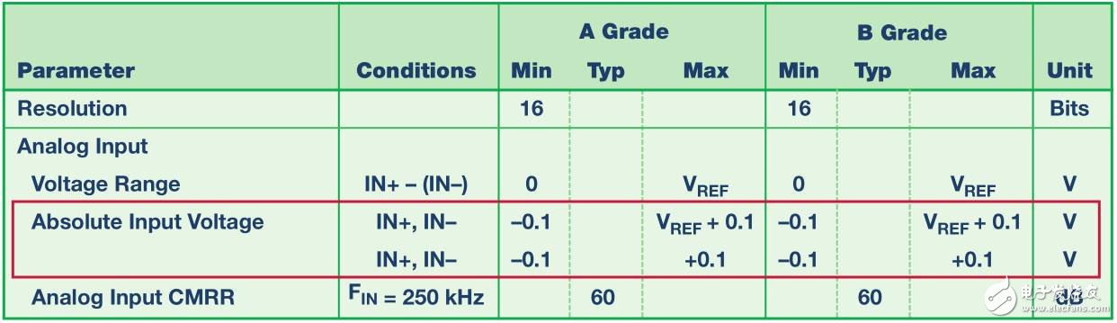
Figure 3. Absolute Input Voltage Example
In some cases, the negative input has a limited range relative to the positive input. While the positive input can swing freely within its allowable range, the negative input may be restricted to a small ± voltage range near the ADC ground. The permissible input range for each ADC pin is detailed in the datasheet under the "Absolute Input Voltage" specification.
If a pseudo-differential device like the AD7980 has a limited IN– voltage range, and it needs to reject large interfering signals beyond that range, an instrumentation amplifier may be necessary before the signal reaches the ADC. There are three pseudo-differential configurations: unipolar, pseudo-bipolar, and true-bipolar. ADI offers devices in each of these categories. Examples include the AD7980 and AD7988-5 for unipolar pseudo-differential inputs.
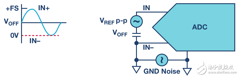
Figure 4. Unipolar Pseudo-Differential
In a unipolar pseudo-differential setup, a single-ended unipolar signal is applied to the positive ADC input, while the source ground is connected to the negative ADC input. This configuration allows for relative measurements without the need for a separate reference ground.
In a pseudo-bipolar configuration, the single-ended signal is still applied to the positive input, but the source ground is not directly connected to the negative input. Instead, it is biased to half the full-scale voltage. This changes the input range to ±VFS/2 instead of 0 to VFS. Although the dynamic range remains the same, the relative voltage at which the positive input is measured differs. Devices offering pseudo-bipolar inputs include the AD7689.
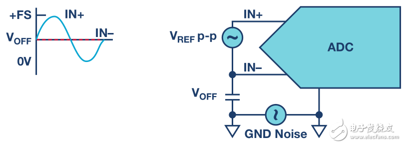
Figure 5. Pseudo-Bipolar
Similar to the unipolar pseudo-differential case, the pseudo-bipolar negative input has a limited range. In this case, the voltage varies from VFS/2 to ground. The diagram above shows the input range for a pseudo-bipolar configuration. Here, VOFF = VFS/2.
The true-bipolar pseudo-differential case is similar to the unipolar version, but the positive ADC input can swing up and down at a low voltage. Typically, the peak-to-peak input range is twice the reference voltage. A device that supports this is the AD7606.
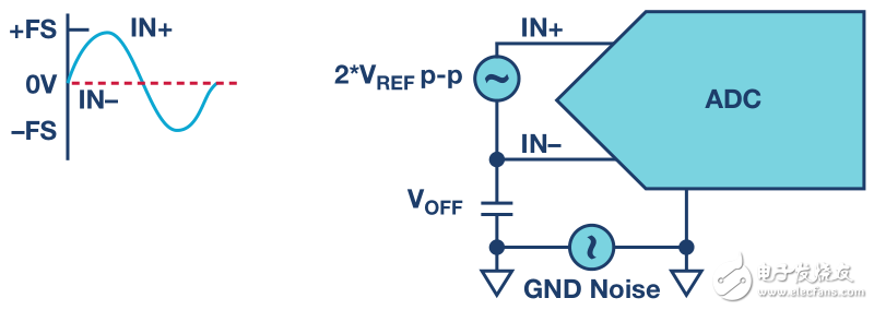
Figure 6. Pseudo-Differential True Bipolar
For instance, if the reference voltage is 5 V, the pseudo-differential true bipolar device can accept inputs ranging from -5 V to +5 V. Figure 6 shows the input range for this configuration.
Differential Input
Compared to single-ended configurations, the pseudo-differential architecture offers better suppression of disturbance signals. However, there are other architectures that provide similar benefits while also increasing the system's dynamic range.
ADI provides two differential input devices. One of them is the differential inverting configuration. In this case, the ADC converts the difference between the positive and negative inputs, which swing 180° out of phase. Most differential inverting devices are unipolar, meaning both sides of the differential signal swing between a low voltage and the positive full scale (determined by the reference). The common-mode voltage is fixed because the two inputs are out of phase. Like pseudo-differential devices, differential inverting devices have a limited common-mode input range, which is specified in the product datasheet. As shown in Figure 7 below, for devices with an absolute input range from 0 V to the positive full scale, the common-mode voltage is VFS/2. For high-resolution (16-bit and above) differential inverting SAR ADCs, the common-mode range is typically ±100 mV.
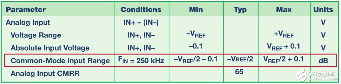
Figure 7. Differential Common Mode Input Range
The differential architecture allows users to maximize the ADC's input range. Compared to single-ended or pseudo-differential setups, differential signaling doubles the input range for a given supply and reference voltage, providing up to 6 dB of dynamic range improvement without increasing power consumption.
When maximum performance is required, a differential inverting device is often selected. The differential signal provides excellent noise rejection and tends to eliminate even-order distortion. As shown in Figure 8, the dynamic range and SNR improve compared to single-ended and pseudo-differential configurations due to the opposing swings of the differential pins.
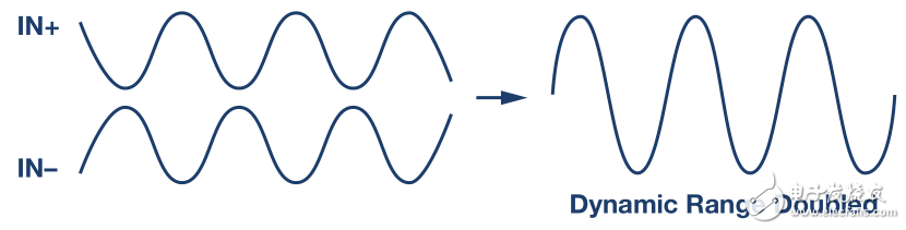
Figure 8. Dynamic Range Increase Due to Differential Signaling
To achieve optimal performance in a single-ended signal chain, a single-ended to differential amplifier, such as the ADA4940-1 or ADA4941-1, can be used to condition the input signal and match its common-mode level to the ADC. Figure 9 shows the differential inverting input range. Devices with differential inverting inputs include the AD7982, AD7989-5, and AD7915.
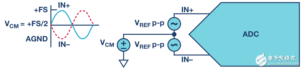
Figure 9. Differential Inversion
As with pseudo-differential devices, if the system has significant common-mode signals, an instrumentation amplifier should be used to condition the input. The differential ADC handles fine variations in the common mode and offers excellent CMRR for the entire signal chain.
Common-mode range limits are essential for achieving optimal performance and avoiding degradation of the converter’s dynamic range. Some common mistakes when using differential inverting devices may violate the common-mode range. Figure 10 shows a typical user error when implementing a differential inverting device. The datasheet for devices that violate the limits in Figure 7 can help avoid such issues.
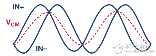
Figure 10. Violation of Common Mode
In this case, the differential signal is not 180° out of phase, causing the common-mode voltage to vary significantly between the two ADC input pins. Another common mistake is having a 180° inverted but improperly biased signal, or connecting the IN– pin of the ADC to a DC bias voltage. Applying a DC voltage to the negative ADC input quickly violates the common-mode range specification, eliminating the dynamic range advantage of the differential signal. The second differential signal measures the difference between any two signals, regardless of their common-mode voltage.
ADI offers a comprehensive range of data acquisition solutions based on SAR ADC technology for measuring fully differential signals. For signal chain designers seeking integrated data acquisition systems with a wide common-mode input range, ADI provides the ADAS3022 and ADAS3023. These are bipolar, continuous, and simultaneous sampling data acquisition systems with a common-mode range of ±10 V, capable of measuring the difference between any two signals within that range.
The analog input type can affect the digital output encoding. Converters with unipolar input ranges, such as single-ended unipolar and pseudo-differential devices, use direct binary encoding. Code 0 represents the negative full-scale input voltage, and code 2^N – 1 (where N is the number of bits) represents the positive full-scale input. Devices with ± polarity inputs use two's complement to provide a sign bit to the user. These include single-ended bipolar, pseudo-differential bipolar, and fully differential devices. For these ADCs, the negative full-scale input is represented by the code –2^(N–1), and the positive full-scale input is represented by the code 2^(N–1) – 1.
in conclusion
The SAR ADC is a versatile, low-power, and high-performance option for creating analog-to-digital conversion signal chains. These devices are straightforward to implement. However, to achieve the desired system performance, specific architectural choices must be made. This article specifically discusses the selection of analog input types offered in the ADI SAR ADC portfolio. Each input type has its own advantages and trade-offs. As mentioned, the right choice is crucial for achieving optimal performance.

Step Down Transformer,Step-Down Transformers,Transformer Step Down,Step-Down Electrical Transformers
Huizhou Show-Grand Electronics Co., Ltd. , https://www.sgtransformer.com