It was still dark when the chicken screeched, and the sun hadn’t fully risen over the horizon. The air was still, and the old shop welcomed its first customer of the day.
The shopkeeper greeted, “It’s really early here—what’s the purpose?â€
“Input devices for the SAR ADC analog input architecture,†the customer replied.
“Do you want a single-ended input, a pseudo-differential input, or a differential input?†the shopkeeper asked.
The customer frowned slightly, “Why so many options?â€
The shopkeeper smiled, “These input types are all available, so let's talk about the entrance…â€

**What is a SAR ADC?**
Successive Approximation Analog-to-Digital Converters (SAR ADCs) are general-purpose ADCs that convert continuous analog signals into discrete digital representations. They do this by comparing a known charge with the input charge through a charge redistribution process. A binary search is performed during the conversion period to find the closest digital code, which brings the internal comparator back to equilibrium. The sequence of 0s and 1s represents the decision made by the circuit, restoring system balance.
SAR ADCs are versatile, easy to use, and asynchronous. However, choosing the right input type for a specific application is essential. This article focuses on the analog input types offered in ADI’s SAR ADC portfolio, but it's important to note that these input types are common across all ADC architectures. Depending on the signal source or the overall design goals, certain trade-offs must be considered. The simplest approach is to match the ADC input type to the source output configuration. But sometimes, signal conditioning might be needed, or cost, power, or area constraints could influence the choice. Let’s explore the different analog input types available.
**Single-Ended Input**
The most straightforward analog input type is the single-ended input. In this case, only one signal line is needed from the source to the ADC. One input pin is used, and there is no return path or ground reference. The conversion result is measured relative to the ADC’s ground pin. Single-ended inputs can be unipolar or bipolar, depending on the device. The main advantage is simplicity: fewer traces mean less complexity and lower power consumption in the signal chain. However, this simplicity comes at a cost. Single-ended systems cannot suppress DC offsets, and voltage differences between the signal source ground and the ADC ground may affect the conversion results. Additionally, they are more susceptible to noise coupling. Therefore, the signal source and ADC should be placed close together to minimize these effects.
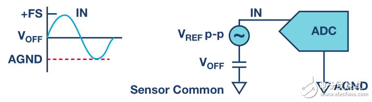
**Figure 1. Single-Ended Unipolar**
In a unipolar single-ended configuration, the signal swing is between ground and the positive full scale, usually defined by the ADC reference voltage. Devices like the AD7091R and AD7091R-8 support this setup.
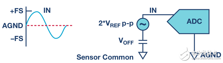
**Figure 2. Single-Ended Bipolar**
For a bipolar single-ended configuration, the signal swings between negative and positive full scale. The AD7656A-1 is an example of such a device.
**Pseudo-Differential Input**
If the signal needs to be referenced independently of the current-carrying path, a pseudo-differential input may be a better choice. It functions like a single-ended ADC but uses a reference ground. The ADC performs a differential measurement, where the sensed voltage is measured relative to the input signal ground. The single-ended signal is applied to the positive input (IN+), while the signal ground is connected to the negative input (IN–). Designers should pay attention to the input range of the negative pin.
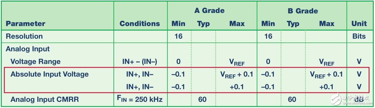
**Figure 3. Absolute Input Voltage**
Some ADCs have limited input ranges for the negative pin relative to the positive. In such cases, the positive pin can swing freely, while the negative pin is restricted to a small ± voltage range near the ADC ground. For example, the AD7980 has a limited IN– range and may require an instrumentation amplifier to reject large common-mode signals before they reach the ADC.
There are three pseudo-differential configurations: unipolar, pseudo-bipolar, and true bipolar. ADI offers devices in each category. The AD7980 and AD7988-5 are examples of unipolar pseudo-differential ADCs.
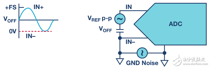
**Figure 4. Unipolar Pseudo-Differential**
In a unipolar pseudo-differential setup, a single-ended unipolar signal is applied to the positive input, and the source ground is connected to the negative input.
In a pseudo-bipolar setup, the source ground is not connected directly to the negative input but instead set to half the full-scale voltage. This allows the input range to be ±VFS/2 instead of 0 to VFS. The dynamic range remains the same, but the relative voltage measurement changes.
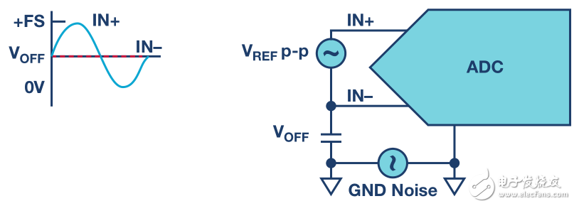
**Figure 5. Pseudo-Bipolar**
The pseudo-bipolar negative input has a limited range, typically from VFS/2 to ground. The AD7689 is an example of a pseudo-bipolar ADC.
In the true bipolar pseudo-differential configuration, the positive input can swing up and down around a low voltage, offering a larger peak-to-peak input range. The AD7606 is an example of a pseudo-differential true bipolar ADC.
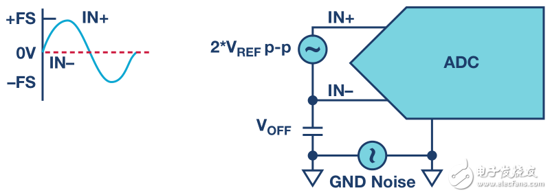
**Figure 6. Pseudo-Differential True Bipolar**
For example, if the reference is 5 V, the AD7606 can accept inputs in the ±5 V range.
**Differential Input**
Differential input architectures offer better noise rejection than single-ended or pseudo-differential designs. They also provide a wider dynamic range. ADI offers two types: differential inverting and fully differential.
In a differential inverting configuration, the ADC converts the difference between the positive and negative inputs, which are 180° out of phase. These devices are typically unipolar, with both inputs swinging between a low voltage and the positive full scale. The common-mode voltage is fixed due to the phase difference. The allowable common-mode input range is specified in the data sheet.
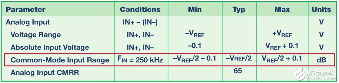
**Figure 7. Differential Common Mode Input Range**
Differential signaling doubles the input range for a given supply and reference setting, providing up to 6 dB of dynamic range increase without increasing power consumption.
When maximum performance is required, a differential inverting device is preferred. It provides excellent noise rejection and reduces even-order distortion. The AD7982, AD7989-5, and AD7915 are examples of differential inverting ADCs.
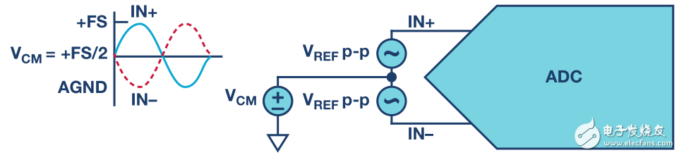
**Figure 9. Differential Inversion**
If the system has a large common-mode signal, an instrumentation amplifier should be used to condition the signal before it reaches the ADC. The differential ADC handles small variations and maintains high CMRR.
Common-mode range limits are critical for optimal performance. Violating these limits can reduce the dynamic range. For example, if the differential signal is not 180° out of phase, the common-mode voltage fluctuates, leading to poor performance.
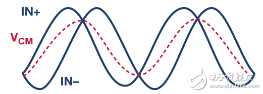
**Figure 10. Violation of Common Mode**
Another common mistake is applying a DC voltage to the negative input, which violates the common-mode specification and eliminates the benefits of differential signaling.
ADI offers comprehensive solutions for fully differential signals, including the ADAS3022 and ADAS3023, which support a wide common-mode range of ±10 V.
Finally, the analog input type affects the digital output encoding. Unipolar inputs use direct binary encoding, while bipolar inputs use two’s complement to represent the sign. This ensures accurate representation of both positive and negative voltages.
**Conclusion**
SAR ADCs are flexible, low-power, and high-performance components for analog-to-digital conversion. While they are easy to implement, achieving optimal system performance requires careful architectural choices. This article discussed the various analog input types available in ADI’s SAR ADC portfolio, highlighting their advantages and trade-offs. Choosing the right input type is crucial for maximizing performance and meeting design requirements.

PFC Inductor,Switch Mode Transformer,PFC Inductor Coil,Toroidal PFC Inductor
Huizhou Show-Grand Electronics Co., Ltd. , https://www.sgtransformer.com