Abstract: This paper studies a high-efficiency double-tube forward DC converter suitable for electric vehicles. On the basis of proposing a design scheme, the key parameters of the control circuit, feedback loop, starting circuit and transformer are emphasized. Detailed analysis of the design. The control circuit uses the SG3525 chip and compensates the control circuit with a type II compensation. The experimental test results show that the converter output is stable and has high conversion efficiency.
Key words: double-tube forward; DC converter; type II compensation; electric vehicle
As a new energy vehicle, electric vehicles have been rapidly developed. The energy of an electric vehicle is generally supplied by a battery pack (voltage 72 V) consisting of 6 batteries in series, but some auxiliary electronic devices in electric vehicles, such as car headlights, brake taillights, horns and wipers, have an operating voltage of 14 V, therefore requires a reliable voltage conversion from a 72 to 14 V DC converter. At the same time, due to the limitation of the working environment inside the electric vehicle and the energy saving point of view, the DC converter must have a high conversion efficiency. According to the actual working requirements of electric vehicles, the designed DC converter adopts a double-tube forward topology with an output power of 300 W and a conversion efficiency of more than 85%. Because the voltage stress of the MOS tube in this design is small, the transformer has a simple structure, does not require a magnetic reset winding, and does not have the problem of straight-through of the bridge arm, so the design is simple and the reliability is high.
1 System structure The structure diagram of the vehicle double-tube forward DC converter is shown in Figure 1.
This article refers to the address: http://
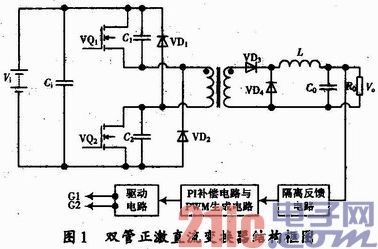
The system consists of four parts: power circuit, isolated feedback circuit, PI compensation circuit and PWM generation circuit and drive circuit. The isolated feedback circuit is mainly composed of an optocoupler P521 and a precision voltage regulator TL431, which isolates the output voltage and feeds it back to the control chip. The PI compensation circuit and the PWM generation circuit are implemented by the chip SG3525. The driving circuit is used to split the PWM signal into two independent signals G1 and G2 for driving the MOS transistors VQ1 and VQ2, respectively. These four parts form a closed-loop system that adjusts the duty cycle based on the output voltage and ultimately stabilizes the output voltage.
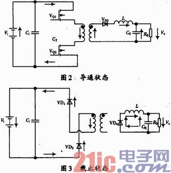
The two operating states of the two-switch forward DC converter operating in current continuous mode can be represented by the following simplified circuit (for ease of analysis, ignoring the turn-on voltage, turn-on voltage drop, and parasitic capacitance of the MOS transistor, simplifying the converter In two working states: switch conduction state and switch closure state):
The working process of the double-tube forward converter is: when the MOS tube is turned on, the primary side current flows through the upper tube VQ1, the transformer primary, and the lower tube VQ2 returns to the negative pole of the battery pack. The excitation current gradually increases during this process. The secondary side rectifier diode VD3 is turned on, the freewheeling diode VD4 is turned off, the battery pack supplies energy to the load through the transformer, and charges the output capacitor. When the MOS transistor is turned off, the two MOS transistors on the primary side are turned off, the excitation diodes VD1 and VD2 are turned on, and the excitation current is gradually decreased to zero, and the transformer is magnetically reset. The secondary side rectifier diode VD3 is turned off, and the freewheeling diode VD4 is turned on, and the electrical energy stored in the inductor supplies current to the load. See Figure 2 and Figure 3.
2 related circuit design
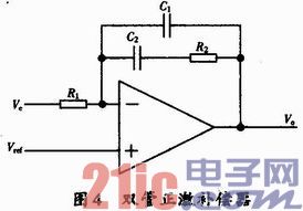
2.1 Control circuit and compensation circuit The control circuit of the double-tube forward converter uses the SG3525 control chip. Compared with other control chips, the SG3525 removes the current-limit comparator and uses the external shutdown signal input to implement the current-limit function. At the same time, it also has pulse-by-pulse shutdown and DC output current limiting function, suitable for output low-voltage high-current converter. In actual use, a current detection signal is connected to pin 10 to limit the output current. The SG3525 also has an undervoltage lockout function. When the chip power supply is less than 8 V, the chip has no PWM signal output, and the converter has no output voltage, thus achieving protection. In order to ensure that the high-frequency transformer in the two-switch forward converter completes the magnetic reset in one cycle, according to the volt-second balance principle of the transformer magnetizing inductance, the duty ratio of the converter must be less than 0.5. The maximum duty cycle of the PWM and the dead time are set by adjusting the timing capacitor CT, the timing resistor RT, and the discharge resistor RD on the periphery of the SG3525. The control circuit uses the PWM control chip SG3 525, and the peripheral circuit is simple. The sawtooth frequency in the circuit is determined by RT, CT and RD, taking CT = 1.5 nF, RT = 5.1 kΩ, RD = 220 Ω. According to the formula f=1/[CT(0.7RT+3RD)], the oscillator output frequency is about 140 kHz, and the PWM signal frequency is about 70 kHz. The soft-start function pin is connected to a 4.7μF capacitor. When the capacitor is fully charged and the SG352's 8 pin is high, the SG3525 will start to work. A stable system requires a loop open-loop BODE plot with a slope of -20 dB/dec at the shear frequency and a phase margin of at least 45°. The dual-tube forward DC converter uses a two-type compensation circuit (see Figure 4) whose transfer function is: 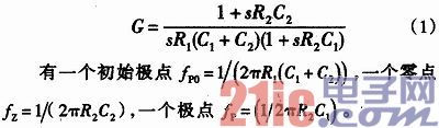
When designing, the crossing frequency is set to 1/4 switching frequency; the zero frequency is set to 1/4 filter resonant frequency, and the mid-band phase margin is increased; the pole frequency is set to 1/4 filter capacitor's own resistance frequency, and the high frequency band is increased. Attenuation. by 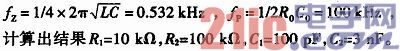
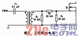
2.2 The two MOS transistors of the double-switch forward circuit of the drive circuit are controlled by the same PWM signal to turn on and off the MOS transistor, but the upper tube of the double-switch forward converter is floating, so it is necessary to isolate the two driving signals. . A dedicated driver chip is usually available, but the driver chip is expensive and less reliable than a transformer driver. One of the converters uses transformer isolation, and the schematic is shown in Figure 5. This method uses fewer devices, lower cost, and higher reliability than the driver chip.
2.3 Feedback Circuit Feedback Circuit As shown in Figure 6, the two-switch forward DC converter uses a voltage feedback control loop to ensure that the output voltage is a stable value under different load conditions. Because the input terminal and the output terminal do not share ground, it needs to be isolated. The optocoupler P521 and the precision voltage regulator tube TL431 are used as reference, isolation, sampling and amplification to form a negative feedback loop. In the secondary circuit, the voltage regulator TL431 acts as a reference and feedback error amplifier, samples the output, and produces the corresponding error voltage. When the forward current If of the optocoupler is less than 5 mA, a slight change of If will cause a sharp change of the triode current Ic; when the forward current If is greater than 10 mA, the optocoupler begins to become saturated, so the static working point of the optocoupler is set at If = 5 ~ 10 mA is more appropriate. When the TL431 is working normally, the cathode voltage is 2.5 V, so R7 takes 1.2 kΩ to ensure that the optocoupler works at a suitable static operating point. There are two factors to consider for the value of R11:
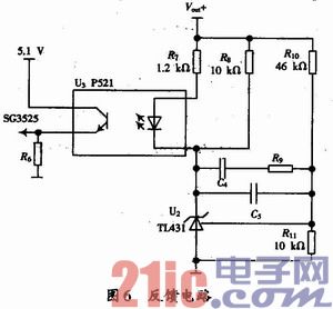
(1) The current of the TL431 reference input. Generally, this current is 2μA. In order to avoid the influence of the current on the terminal voltage and the noise, the current flowing through the resistor R11 is generally more than 100 times of the reference current, so the resistance is less than 12.5 kΩ.
(2) Loss requirements. In the case of less than 12.5 kΩ, the larger the resistance, the smaller the loss, so R11 takes a value of 10 kΩ.
According to the performance of TL431, R10, R11, Vo, vr have a fixed relationship:
Vo=(1+R10/R11)Vr (2)
Where: Vo is the output voltage; Vr=2.50 V is the reference voltage, so R10 takes 46 kΩ.
The minimum cathode current of the TL431 is 0.2 mA. To ensure proper operation of the TL431, the wind provides the minimum cathode current for the TL431. Since the TL431 has a minimum cathode voltage of 2.5 V and an output voltage of 14 V, R8 takes a value of 10 kΩ to ensure a minimum cathode current.
2.4 Startup Circuit The startup circuit is shown in Figure 7. The function of the startup circuit is to supply current to the PWM modulation chip supply pin when the converter starts operating. When the converter starts normal operation, the power supply circuit supplies power to the chip, and the startup circuit is disconnected.
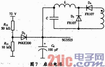
When the DC converter is powered up, the anode voltage of the diode D2 is 12 V under the action of the voltage dividing resistor. Current flows through diode D2 to supply current to the chip supply pin. After the chip starts working, it outputs the maximum duty cycle and drives the MOS transistor. The power supply circuit starts to work, outputting 16 V voltage, higher than the diode anode voltage, the diode is disconnected, and the startup circuit is no longer working.
3 The design of the key parameters of the converter and the choice of the device In the DC converter, the calculation of the transformer and the output inductance parameters directly determine the reliability and efficiency of the double-switch forward converter, and the choice of the MOS tube and the secondary rectifier freewheeling diode It also has an impact on converter conversion efficiency.
3.1 Selection of transformer core The calculation method of core size generally includes area multiplication method (AP method) and magnetic core geometric parameter method (KG method). Here, area multiplication method is used, and the calculation formula is as follows: ![]()
Where: Aw is the core copper window area (unit: cm2); Ae is the effective cross-sectional area of ​​the core (unit: cm2), PT is the apparent power of the transformer (unit: W); △ B is the magnetic induction intensity increment ( Unit: T); fs is the operating frequency of the transformer (unit: Hz); J is the current density <unit: A/cm2), depending on the heat dissipation method, 300 to 600 A/cm2 may be taken, and Ku is the copper window occupancy factor.
The transmission efficiency of the converter is set to 85%, the maximum duty ratio is 0.4, and Ku=0.2. Calculate AP=3.15 cm4 according to formula (3), and use EE type core EE42/42/20.
3.2 Design of transformer parameters In a two-switch forward DC converter, the maximum duty cycle should be less than 0.5. First assume that the maximum duty cycle Dmax1 = 0.4, by the formula: 
Calculate the primary number of turns is 12åŒ, then the number of secondary turns is 6åŒ. The maximum variation of the magnetic flux density in the magnetic core ΔB=0.188<0.25, which ensures that the magnetic core does not saturate.
3.3 Output Inductor Design The output of the dual-tube forward converter operates in current continuous mode. The required inductance is: ![]()
Where: V1 is the input voltage of the inductor; D is the duty cycle; f is the switching frequency; Io is the output current; k=â–³I/2I is the ripple coefficient, generally 0.05. In this system, the inductor input voltage is 36 V, the maximum duty cycle is 0.388, the switching frequency is 70 kHz, and the output current is 22 A. The minimum inductance required can be calculated by equation (3): ![]()
Considering that the inductance is reduced after the inductor is biased, the output current ripple is increased, and the load of the output capacitor is increased. The actual value of the inductor is 90 μH.
3.4 MOS tube and diode selection converter When operating at full load, the average input current is 5 A and the peak current is 7.5 A. When the converter is operating in the off state, the MOS tube is subjected to a voltage stress of 72 V. Consider the IR model IRFP250 and IRFP260, both of which have a breakdown voltage of 200 V and can withstand a voltage stress of 72 V. The IRFP250 has a maximum on-current of 30 A, an on-resistance of 0.075 Ω, and a conduction loss of 4.22 W at full load. The IRFP has a maximum on-current of 50 A, an on-resistance of 0.04 Ω, and a conduction loss of 2.25 W at full load. The IRFP260 is selected from the viewpoint of conduction loss and temperature rise of the MOS tube. When the converter is operating at full load, the output current is 22 A. The secondary rectification and freewheeling diodes use Schottky diode 30CPQ100, which has a maximum forward conduction current of 30 A and a small on-state voltage drop of 0.67 V, which is suitable for use as a secondary rectification and freewheeling diode.
4 Circuit debugging and performance analysis According to the above parameters, a prototype of a two-switch forward converter is developed. During the debugging process, the following problems will be encountered:
(1) SG3525 does not work at first. The SG3525's supply current can be increased by reducing the startup circuit, and this parameter can be changed to work properly.
(2) The output voltage is unstable at no load. A resistor can be connected in parallel with the output as a dummy load, but there is a loss; in addition, the capacitance in the PI compensation circuit can be changed to improve the transient response of the system.
(3) The output voltage drops when the load increases. The reason is that the maximum duty ratio in the actual circuit does not reach the designed value. The RD resistance of the SG3525 can be adjusted to adjust the maximum duty ratio to stabilize the output voltage at 14 V. .
The actual circuit has been tested. The maximum duty cycle is 37.77% at full load, the output voltage is 13.64 V, the output current is 21.8 A, and the conversion efficiency is 85.71%. The measured waveform of the converter at full load is as follows. Figure 8 shows.
The rising edge of the PWM signal is less than the falling edge time because there is a small parasitic capacitance between the source and the drain of the MOS transistor. When the MOS transistor is turned off, the wife needs to charge the parasitic capacitance. The upper tube has a burr when it is turned on because the upper tube drive has a burr at the rising edge.
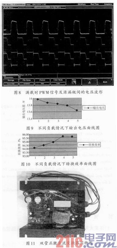
Under different load conditions, the output voltage and conversion efficiency of the converter are shown in Figure 9 and Figure 10, respectively. It can be seen that the conversion efficiency will change with the output voltage value: when the load increases, the output voltage decreases. The efficiency is gradually increased, but the efficiency is reduced at the maximum load. The reason is that the power consumption of the control circuit is a certain amount. It is assumed that the sum of the impedances of the primary winding of the transformer and the on-resistance of the MOS transistor is Rp, and the sum of the impedance of the inductance and the secondary winding of the transformer is Rs, and the total loss is: ![]()
As the load increases, the loss rises exponentially; the conversion efficiency reaches a maximum at a certain value of the output current and then begins to fall. The completed physical diagram of the vehicle double-tube forward DC converter is shown in Figure 11. For safe and reliable operation, the outer casing of the converter adopts a fully enclosed aluminum alloy structure, and the circuit board is also filled with silica gel to increase the converter. Heat dissipation and shock resistance.
5 Conclusion This vehicle dual-tube forward DC converter has been used in batches on electric vehicles produced by an electric vehicle company. After long-term operation, its operation is stable, output voltage precision is high, output current is large, and conversion efficiency is high. Good economic and social benefits.
Usb Charger Cable advantage:
For iPhone Cable Charger High Quality Usb Data Line 2.1A Fast Charging USB Cable For Apple Charging Chord For phones Charger
100% Brand new and high quality.Feel smooth, tough and durable,Original quality cable for smart phone.Set bracket, lightning charging solid data line, copper wire specifications, charging 2 core *25*0.1, data 2 core *12*0.1 74 copper wire.

Usb Charger Cable,Usb Charging Cable,Usb Cable Charging Cable,Micro Usb Charger Cable
Dongguan City Leya Electronic Technology Co. Ltd , https://www.dgleya.com