Power efficiency is important for the noise immunity of portable devices and analog ICs. This article focuses on the voltage reference circuit, which not only supports very low operating quiescent current (less than 250nA), but also conforms to standard CMOS processes. Optimized for a wide range of applications, this circuit is suitable for portable electronic devices, automotive, medical devices, and system-on-a-chip (SoC) implementations where high power supply rejection ratio (PSRR) and switching noise immunity are important.
The above voltage reference supports 90dB at low frequencies. The standard deviation of the output voltage variation is 0.5%, and the temperature coefficient is -15ppm/°C over the -40°C to 125°C temperature range. These features are available from a supply voltage range of 1.6V to 5.5V. Various methods for achieving input noise immunity for voltage references can be implemented.
Introduction
Almost every analog circuit requires a high-precision, high-stability reference or current source. However, the reference voltage module should not be a limiting factor when choosing system-on-chip (SoC) technology. That is to say, the technical process selected for this type of system is not always optimal for the reference voltage source. Therefore, its design should be more stable in order to adapt to changes in various technological processes.
The battery is usually used as a power source for the SoC. This further increases the linear regulation performance of the voltage reference source operating over a large supply voltage range. To extend battery life, a low quiescent supply current is required. At the same time, high power supply rejection ratio (PSRR) is required at a wide frequency to suppress noise from high speed digital circuits, buck converters, or other switching circuits on the chip. This article focuses on an ultra-low quiescent current bandgap voltage reference with high PSRR.
Basic bandgap voltage reference structure
The main idea for improving PSRR is to place a bandgap voltage source behind a low dropout regulator (LDO). Existing linear regulator topologies vary widely in quiescent current, DC load regulation, transient response, decoupling capacitance, and silicon area requirements. Since our goal is to provide a fully integrated LDO on the same chip without external capacitors, a typical LDO structure is not suitable.
These structures contradict the ultra-low quiescent supply current. To alleviate this contradiction, you can use the same bandgap as the reference source for the LDO. The reason why the standard LDO structure should not be used is that it requires an output capacitor for stable operation. The best option is a structure with a gain stage that is stable without the need for an output capacitor.
Low dropout regulator
Figure 1 is a simplified diagram of the core of the LDO used in the design [1]. M0 and M4 in Figure 1 [2] represent the Inverted Voltage Follower (FVF), which implements a single-stage regulation with no reverse function and associated poles. The quiescent current is determined by transistors M1 and M3. Transistor M2 can function as a common-gate amplifier.
The open loop gain of the LDO is determined by the first cascade stage (ie, transistors M 2 and M3). There is a low impedance source for the M4 PMOS follower that acts as a load, so the output gain of FET M0 is close to 1. With the help of the small signal equivalent circuit in Figure 2, the stability analysis of the proposed LDO structure shows that there is only one pole (Equation 1):
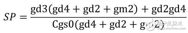
The M0 gate source capacitor, which acts as a compensation capacitor, creates the main pole of the LDO. Therefore, the LDO [3] can be stabilized without the need to decouple the off-chip capacitors.
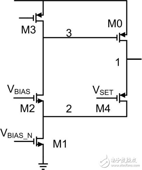
Figure 1. LDO with flip voltage follower and no output capacitor
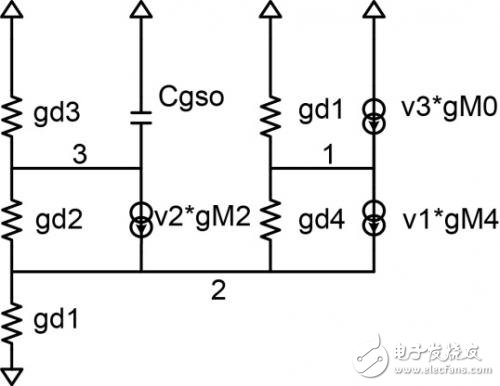
Figure 2. Small Signal Equivalent Circuit of LDO
Another advantage of this LDO is the simple self-starting program, which does not require dedicated circuitry. Initially, when the voltage VDD is 0, VOUT is also 0, the follower M4 is turned off without feedback, and the bias current of M1 is greater than the bias current of M3. Therefore, the gate voltage M0 can be reduced not only, but also the output voltage VOUT can be driven to the selected output voltage value.
The disadvantages of this architecture are line regulation and poor PSRR. The reason is the low open loop gain because it is determined by only one gain stage. A reasonable solution might be the first stage cascading current source, which increases the gain, which in turn increases line regulation performance and PSRR.
The LDO output voltage in Figure 1 is (Equation 2):
![]()
Among them, VSET is the reference voltage, VGS, M4 is the gate-source voltage of M4.
Therefore, the output voltage is extremely sensitive to temperature and process variations. To avoid this problem, you must create a more ideal follower, where M4 is part of the feedback loop (Figure 3).
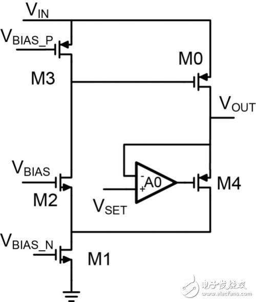
Figure 3. M4 LDO with no output capacitor in the amplifier feedback loop.
The output voltage in this case is Equation 3:
![]()
Among them, A0 is the open loop gain feedback of the amplifier. For high feedback amplifier gain, Equation 4 can be used:


Figure 4. LDO with resistive divider, M4 in amplifier feedback loop, no output capacitor
After adding a resistive voltage divider to the feedback loop (Figure 4), the output voltage is converted to:
VOUT=VSET(1+R1/R2)
The FVF feedback amplifier does not affect the overall LDO stability because it is external to the main LDO feedback loop. For the local feedback loop, only the design solution is required to be stable.
Bandgap kernel description
The bandgap core chosen (Figure 5) uses a classic architecture that is widely used in standard CMOS technology.

Figure 5. Simplified block diagram of the recommended bandgap voltage reference core
The low temperature coefficient of the bandgap voltage can be obtained by adding the negative temperature coefficient base-emitter voltage of the bipolar transistor, so that the positive temperature coefficient voltage can be obtained by the difference between the voltages of the two base emitters biased at different current densities. . To select equal values ​​for resistors R2 and R3, the reference voltage can be expressed as Equation 5:
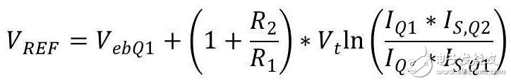
Where VEB is the base-emitter voltage of Q1, VT is the thermal voltage, IQ1 and IQ2 are the currents through transistors Q1 and Q2, and IS, Q1 and IS, and Q2 are the saturation currents of Q1 and Q2, respectively.
filter,cylinder,solenoid valve
Wuxi Trenty Machinery & Equipment Co., Ltd. , https://www.elec-inverter.com