Sensor excitation
Sensors are everywhere, they are used to measure temperature, light, sound and various other environmental parameters. The output voltage or current of some sensors depends on certain physical parameters. For example, a thermocouple produces a voltage that is proportional to the temperature difference between the reference junction and the measurement point. The transfer function of most sensors follows a known relationship with respect to physical parameters. The transfer function is usually an impedance, the current is the sensor input, and the voltage across the sensor represents the target parameter. Resistive sensors (such as load cells, RTDs, and potentiometers) are used to measure stress, temperature, and angle, respectively. In the first order, the resistive sensor is frequency independent and has no phase response.
Many sensors require an AC excitation signal because their transfer function varies with frequency and phase. Examples of such are inductive proximity sensors and capacitive humidity sensors. Bioimpedance measurements can capture respiratory rate, pulse rate, hydration, and various other physiological parameters. In these cases, the magnitude, phase (or both) can be used to determine the value of the test parameter.
In some applications, the sensor can convert the sample to be tested into a sensor. For example, a colorimeter uses an LED to illuminate light through a sample of liquid to be tested. The light absorption of the sample modulates the amount of light detected by the photodiode to reveal the characteristics of the liquid to be tested. The blood oxygen content can be determined by measuring the difference between red light and infrared light absorption in vascular tissue. The ultrasonic sensor measures the gas flow rate based on the Doppler shift of the ultrasonic travel in the gas. All of these systems can be implemented by synchronous demodulation.
Figure 1 shows a synchronous demodulation system that measures the sensor output signal. The excitation signal fx is used as a carrier, and the sensor is modulated with amplitude, phase (or both) as a function of the parameter to be measured. The signal may be amplified and filtered, and then modulated down by the phase sensitive detector (PSD) to return to DC. The output filter (OF) limits the signal bandwidth to the frequency range of the parameter to be tested.
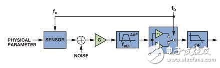
Figure 1. Synchronous demodulation system
The noise at the sensor output may be affected by internal source or external coupling. Low frequency (1/f) noise often limits the performance of sensors or measurement electronics. Many sensors are also susceptible to low frequency ambient noise. Optical measurements are susceptible to background illumination; electromagnetic sensors are susceptible to power supply radiation. Free choice of the excitation frequency to avoid the noise source is an important advantage of synchronous demodulation.
Choosing an excitation frequency that reduces the effects of these noise sources is an important way to optimize system performance. The selected excitation frequency should have a low noise floor and be far enough away from the noise source to properly filter to reduce the noise to an acceptable level. Sensor excitation is usually the largest piece of power budget. If the sensor's sensitivity to frequency relationship is known, then stimulating the sensor at a higher sensitivity can reduce power consumption.
Phase sensitive detector
To understand the requirements of anti-aliasing filters (AAF) and OF, you need to understand PSD. Consider expanding the input signal by +1 and –1 times the PSD by the excitation signal. This is equivalent to multiplying the input signal by a square wave of the same frequency. Figure 2a shows the time domain waveforms of the input signal, voltage reference, and PSD output; in the figure, the input signal is a square wave and any phase is related to the reference voltage source.
When the input and reference voltage have no phase shift at all, the relative phase is 0°, the switching output is DC, and the PSD output voltage is +1. As the relative phase increases, the switching output becomes a square wave twice the reference frequency, and the duty cycle and the mean decrease linearly. When the relative phase is 90°, the duty cycle is 50% and the average value is 0. At 180° relative phase, the PSD output voltage is –1. Figure 2b shows the average PSD output value when the relative phase is scanned from 0° to 360°. The input signal is a square wave and a sine wave.

Figure 2. (a) PSD time domain waveform (b) PSD output average as a function of relative phase
The sine wave case is not as intuitive as the square wave case, but can be calculated by multiplying item by item and decomposing into addition and subtraction terms as follows:
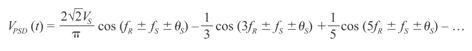
As expected, the PSD generates a proportional response to the cosine of the phase relative to the input signal at the fundamental frequency, but it also produces a response to all odd harmonics of the signal. If the output filter is considered part of a phase sensitive detector, the signal path looks like a series of bandpass filters centered on the odd harmonics of the reference signal. The bandwidth of the bandpass filter is determined by the bandwidth of the lowpass output filter. The PSD output response is the sum of these bandpass filters, as shown in Figure 3. The response portion that appears on the DC side falls within the passband of the output filter. The portion of the response that occurs at the even harmonic of the reference frequency will be suppressed by the output filter.
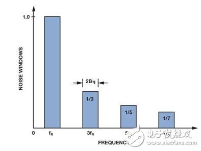
Figure 3. Signal input spectrum that contributes to PSD output
At first glance, the infinite summation of harmonics into the passband of the output filter seems to invalidate this approach. However, since each harmonic term is multiplied and the harmonic noise is added in the square root of the sum of squares, the effect of noise aliasing is alleviated. Assuming that the noise spectral density of the input signal is constant, then the noise effects of harmonic aliasing can be calculated.
Make Vn the integral noise of the transmission window centered on the fundamental frequency. The total RMS noise VT is:
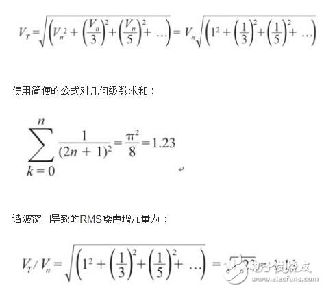
Therefore, the RMS noise generated by all harmonic windows increases the total noise by only 11% (or 1 dB). The output is still susceptible to the passband ripple of the bandpass filter, and the harmonic distortion of the sensor or electronics prior to the PSD will cause an error in the output signal. If these harmonic distortion terms are too large to be acceptable, you can use an anti-aliasing filter to drop them. Anti-aliasing and output filter requirements will be considered in the next design example.
LVDT design example
Figure 4 shows a synchronous demodulation circuit that extracts position information from a linear variable displacement transformer (LVDT, a special winding transformer with an active core attached to the position to be tested). An excitation signal is applied to the primary side. The secondary side voltage varies proportionally to the core position.
There are many types of LVDTs, and the methods for extracting location information are also different. The circuit uses a 4-wire mode LVDT. The secondary outputs of the two LVDTs are connected to their opposite voltages to perform the subtraction. When the LVDT core is at the zero position, the voltage on the secondary side is equal and the voltage difference across the winding is zero. As the core moves from the zero position, the voltage difference across the secondary winding increases. The LVDT output voltage sign changes depending on the direction. The LVDT selected in this example measures ±2.5 mm full-scale core displacement. The voltage transfer function is 0.25, which means that the differential output per volt applied to the primary side is equal to 250 mV when the core is off center 2.5 mm.

Figure 4. Simplified LVDT position detection circuit
Integrated synchronous demodulator
The ADA2200 integrated synchronous demodulator uses a unique charge sharing technique to perform discrete time signal processing within the analog domain. The device's signal path consists of an input buffer, an FIR decimation filter (for anti-aliasing filtering), a programmable IIR filter, a phase sensitive detector, and a differential output buffer. Its clock generation function synchronizes the excitation signal with the system clock. Programmable features are configurable via an SPI-compatible interface.
Figure 5. ADA2200 Synchronous Demodulator
The 4.92 MHz clock generated by the AD7192 24-bit Σ-Δ ADC is used as the host clock. The ADA2200 generates all the internal signals needed for the filter and PSD clock, and also generates an excitation signal on the RCLK pin. The device divides the host clock by 1024 to generate a 4.8 kHz signal and control the CMOS switch. The CMOS switch converts the low noise 3.3 V source to the square wave excitation signal of the LVDT. The 3.3 V supply for the excitation source is also used as the ADC reference, so any drift in the voltage source does not degrade the measurement accuracy. At full-scale displacement, the LVDT outputs a 1.6 V pp output voltage.
Anti-aliasing filter
The RC network between the LVDT output and the ADA2200 input provides low-pass filtering of the LVDT output signal while producing the relative phase shift required to maximize the demodulator output signal. As previously mentioned, Figure 2b shows that the maximum PSD output occurs at a relative phase shift of 0 or 180 degrees. The ADA2200 has 90° phase control so that a ±90° relative phase offset can also be used.
The signal energy of an odd multiple of the demodulation frequency will appear in the passband of the output filter. The FIR decimation filter implements anti-aliasing filtering to provide at least 50 dB of attenuation for these frequencies.
The IIR filter provides additional filtering or gain if needed. Since the IIR filter is in front of the phase sensitive detector, its phase response will affect the PSD signal output bandwidth. This must be considered when designing the filter response.
Output filter
The passband of the output filter should be chosen to match the bandwidth of the parameter under test, but to limit the system's wideband noise. The output low-pass filter must also be able to reject the output spurs generated by an even multiple of the PSD.
This circuit uses the LPF built into the AD7192 of the Σ-Δ ADC. It can be programmed to achieve a sinc3 or sinc4 response, and the transfer function is zero at multiples of the output data rate.
Setting the output data rate of the ADC to the demodulation frequency suppresses the PSD output spurs. The programmable output data rate of the ADC is used as an optional bandwidth output filter. The available output data rate (fDATA) is 4.8 kHz/n, where 1 ≤ n ≤ 1023. Therefore, the ADC averages the modulator output for n demodulation clock cycles for each output data value. Since the master clock is synchronized with the ADC clock, the zero point of the ADC output filter transfer function will fall directly on each harmonic of the modulation frequency and reject all output spurs of any n value.
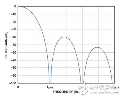
Figure 6 shows the sinc3 transfer function normalized to the ADC output data rate.
The programmable output data rate has an intuitive trade-off between noise and bandwidth/settling time. The output filter noise bandwidth is 0.3 & TImes; fDATA, 3 dB frequency is 0.272 & TImes; fDATA, settling time is 3/fDATA.
At output data rates up to 4.8 kHz, the ADC digital filter has a 3 dB bandwidth of around 1.3 kHz. In the range not exceeding this frequency, the RC filter between the demodulator and the ADC is relatively flat, minimizing the bandwidth requirements of the ADC. In systems with lower maximum data rates, the RC filter corner frequency can be scaled down.
Noise performance
The output noise of this circuit is a function of the ADC output data rate. Table 1 shows the number of significant digits of digitized data relative to the ADC sample rate, assuming a full-scale output voltage of 2.5 V. The noise performance is independent of the LVDT core position.

Table 1. Relationship between noise performance and bandwidth
If the ADA2200 output noise is independent of frequency, then the expected number of significant bits will increase by one bit every 4 & TImes; ENOB does not rise too much at lower output data rates due to the 1/f noise of the ADA2200 output driver; this noise becomes a major component of the noise floor at lower output data rates.
Linearity
The linearity result can be measured by first performing a two-point calibration at a ±2.0 mm core displacement. From these measurements, the slope and offset can be determined to achieve the best straight line fit. The core displacement is then measured over a ±2.5 mm full scale range. The linearity error can be determined by subtracting the measured data from the straight line data.
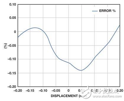
Figure 7. Relationship between position linearity error and LVDT core displacement
E Series LVDT linearity ratings for circuit evaluation are ±0.5% (±2.5 mm displacement range). Circuit performance exceeds LVDT specifications.
Power consumption
The total power consumption of the circuit is 10.2 mW, including 6.6 mW driving the LVDT and 3.6 mW of the rest of the circuit. The circuit SNR can be improved by increasing the LVDT excitation signal, but at the cost of higher power consumption. Alternatively, the LVDT excitation signal can be reduced to reduce power consumption while a low power dual op amp is used to amplify the LVDT output signal to preserve the SNR performance of the circuit.
in conclusion
Synchronous demodulation can solve the characteristic challenges common to many sensor signal conditioning. Systems with excitation frequencies below 1 MHz and dynamic range requirements of 80 dB to 100 dB can use low-cost, low-power analog circuits; this method requires very little digital post-processing. Understanding the working principle of the phase sensitive detector and the noise characteristics at the output of the sensor are key to determining the system filter requirements.
Iphone Usb Flash Drive,Usb Memory Flash Stick,4 In 1 Otg Usb Flash Drive,Usb Flash Drive For Iphone
Shenzhen Konchang Electronic Technology Co.,Ltd , https://www.eclinusb.com