With the rapid development of electronic technology, the car reversing assist system has also undergone tremendous changes. At present, ultrasonic reversing radars have been installed in mid- to high-end cars to help drivers monitor the distance between the rear of the vehicle and the obstacles behind the vehicle. However, due to the propagation characteristics of the ultrasonic waves, the reversing radar has a false report on the thin rod-shaped obstacles behind the vehicle. phenomenon. Some manufacturers have tried to integrate the car video rearview mirror with the reversing radar to observe the situation behind the car and display the data measured by the reversing radar to compensate for the lack of performance of the traditional reversing radar. The core of the integration of video rearview mirror and reversing radar is the design of video character superimposer. Due to the complex structure of traditional video character adder, the reliability is poor in the vehicle environment, resulting in high failure rate and high cost of the integrated visual reversing radar. Failed to promote in the market. Therefore, a reversing radar system designed by the new video character display chip MAX7456 is proposed. This system greatly simplifies the design of the video character adder, effectively overcomes the shortcomings of the traditional video character adder and improves the reliability of the system. , reducing system costs. If the camera system of the reversing radar is slightly improved, functions such as video zooming and night vision can be expanded, which has a good market prospect.
1 Introduction to the MAX7456 The MAX7456 is a dedicated video character overlay chip from MAXIM. The device integrates all the functions needed to generate a user-defined OSD and insert it into a video signal, ie, input clamp circuit, sync separator, video timing generator, OSD insertion multiplexer, EEPROM, display memory The OSD generator, clock crystal oscillator and SPI communication interface are integrated into the chip. The user only needs to connect a 27 MHz crystal oscillator and a small number of RC components to form a complete video character adder. For user convenience, the MAX7456 internal character memory is preloaded with 256 characters and graphics for the user to call. The MAX7456 displays a character size of 18x12 pixels and displays up to 16 lines x 30 columns = 480 characters on the screen. When there is no video signal input, the MAX7456 can generate internal video signals to ensure normal subtitle display. The contents of the character memory can be modified through the SPI interface to meet user needs.
1.1 Ports and Functions The MAX7456 is available in a 28-pin package. The port functions can be divided into video signal ports, control signal ports, and auxiliary ports. The functions of each port are described below:
1) The video signal input and output ports of the MAX7456 are VIN and VOUT. The VIN port can receive standard NTSC or PAL video signals. The input video signal is output by the VOUT terminal after the display of the character signal is inserted in the MAX7456.
2) The control signal port of the MAX7456 includes ![]() , SDIN, SCLKSDOUT. SDIN and SCLK are SPI serial data and serial clock ports for setting the operating mode and OSD data of the MAX7456.
, SDIN, SCLKSDOUT. SDIN and SCLK are SPI serial data and serial clock ports for setting the operating mode and OSD data of the MAX7456. ![]() For the chip select signal, SDOUT is the serial data output port.
For the chip select signal, SDOUT is the serial data output port.
3) MAX7456 auxiliary port has CLKOUT, LOS, ![]() ,
, ![]() And SAG. The CLKOUT port is used to clock the other MAX7456s in multiple OSD systems to reduce system cost. LOS is the line sync loss port,
And SAG. The CLKOUT port is used to clock the other MAX7456s in multiple OSD systems to reduce system cost. LOS is the line sync loss port, ![]() Is the line sync pulse output port,
Is the line sync pulse output port, ![]() It is a field sync pulse output port. These three signals are mainly used for system synchronization. The SAG port is connected to a voltage attenuation correction capacitor to reduce the capacity of the output capacitor. Reduce the field tilt.
It is a field sync pulse output port. These three signals are mainly used for system synchronization. The SAG port is connected to a voltage attenuation correction capacitor to reduce the capacity of the output capacitor. Reduce the field tilt.
1.2 Memory read and write timing and configuration
1.2.1 Character Control Principle The MAX7456 uses character memory (NVM) to store dot matrix information for displaying characters. Each character is 18 rows × 12 columns, and the dot matrix addressing order is from left to right, top to bottom. , a total of 216 pixels. Each pixel is described by 2 bits per pixel: 00 for black, 10 for white, X1 for transparent (external synchronization mode) or gray (internal synchronization mode) (X stands for arbitrary value), so 4 pixels can be stored per byte The information requires a total of 54 bytes of storage space per character. For convenient addressing, each 64-byte memory space in the character memory is set to 1 character memory location, where the first 54 bytes store 1 character dot matrix information, and the remaining 10 bytes are unused. The MAX7456 provides a total of 256-character memory cells. These memory cells have been shipped with common numbers, English uppercase and lowercase letters, partial Japanese characters, Chinese characters, and a small number of graphics for users to use. If the user needs to display a custom character or graphic, it is only necessary to input the dot matrix of the custom character or graphic into the character storage unit of the corresponding address through the SPI serial interface to replace the original character dot matrix.
The MAX7456 uses display memory (SRAM) to store the display characteristics of characters on the screen. The MAX7456 divides the screen display into 16 rows x 30 columns (PAL, NTSC 13 rows x 30 columns) for a total of 480 display positions. The display location is addressed from left to right and top to bottom. The address addressing of the display memory is in one-to-one correspondence with the screen display position, so the display memory has a total of 480 storage units, each storage unit has 2 bytes, and the upper byte stores the storage unit address of the displayed character in the character memory (NVM). The lower byte stores the attribute status bits of the displayed character. If the user needs to display a specific character at a certain position on the screen, only the storage unit address in the character memory (NVM) of the specific character in the display memory unit corresponding to the corresponding location is stored in the high byte of the display storage unit. , the status attribute of the displayed character is stored in the low byte, and then the OSD display is turned on.
1.2.2 Display Memory Configuration To properly display the desired content on the screen, the display memory must be properly configured. The memory is controlled by a mode register (DMM), an address high register (DMAH), an address low register (DMAL), and a data input register (DMDI). The configuration process includes: setting the communication working mode through the mode register; selecting the display unit through the address register (DMAH, DMAL); passing the DMAH[1] bit of the address register (note: the data format is "register name [bit])") and the data The input register DMDI configures the selected display memory location. In the 8-bit working mode, the character "C" (NVM memory cell address is 0Dh) is displayed in the second column and the second column of the screen (the display address is 1 Fh), and the configuration process of the display memory through the SPI is explained.
1) Write mode register: DMM[6]=1, select 8-bit working mode;
2) The write address register DMAH[1]=0 sets the data written to the data input register (DMDI) to be the memory location of the displayed character in the display memory (NVM);
3) Write the highest bit address "Ob" of the character display position to the address register DMAH[0];
4) Write the lower 8-bit address "00011111b" of the character display position to the address register DYL[7:0]; display the memory location of the memory by DMAH[0]+DMAL[7:0], a total of 512 addresses Therefore, 9 bit address bits are required, and the MAX7456 uses the first 480 addresses;
5) Write the memory cell (NVM) address "00001101b" of the displayed character "C" to DMDI[7:0], which will be stored in the display memory high of the DMAH[0]+DMAL[7:0] address location. Byte
6) Write address register DMAH[1]=1, set the data written to the data input register (DMDI) to be the character attribute byte of the displayed character;
7) Write the highest bit address "0b" of the character display position to the address register DMAH[0];
8) Write the lower 8-bit address "00011111b" of the character display position to the address register DMAL[7:0];
9) Write the character attribute byte "LBIXXXXXb" of the displayed character to DMDI[7:0], which will be stored in the lower byte of the display memory of the MAH[0]+DMAL[7:0] address location. Where: L is the local background color control bit, L=0 is transparent, L=1 is gray; B is the flicker control bit; I is the inverse color control bit, I=0 is the normal display, and I=1 is the reverse color display; X is an unused bit;
10) Write the video mode register VMO[3]=1 to enable OSD image display.
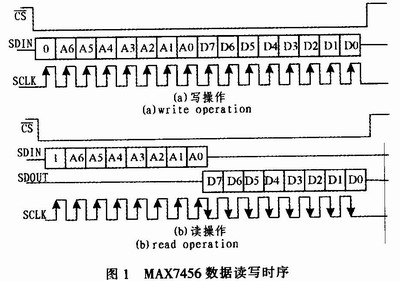
1.2.3 Memory Read and Write Timing The configuration of the MAX7456 display memory (SRAM) and character memory (NVM) is implemented online through the SPI interface. Via SPI interface ![]() The three signals, SDIN and SCLK, can cooperate with each other to read and write the MAX7456 internal registers, and then configure the display memory (SRAM) and character memory (NVM) through registers. Figure 1 shows the MAX7456 data read and write timing. Chip select signal during one operation cycle
The three signals, SDIN and SCLK, can cooperate with each other to read and write the MAX7456 internal registers, and then configure the display memory (SRAM) and character memory (NVM) through registers. Figure 1 shows the MAX7456 data read and write timing. Chip select signal during one operation cycle ![]() After going low, the first byte input through SDIN is the register address. When the highest bit is 0, it is a write operation. When the highest bit is 1, it is a read operation; the second byte is data. There are two exceptions to this format:
After going low, the first byte input through SDIN is the register address. When the highest bit is 0, it is a write operation. When the highest bit is 1, it is a read operation; the second byte is data. There are two exceptions to this format:
1) Auto-increment write mode, which is used to access the display memory and is an 8-bit operation. The display start address must be written to the display address registers DMAH and DMAL before writing data. Then execute the auto-increment write command to the display memory (DMM[6]=1, DMM[0]=1). At this time, the 8-bit increment address is internally generated. SDIN only needs to transfer 8 bits of data per operation cycle until the transfer. The MXA7456 reception is terminated when the value is Oxff.
2) When reading character data from the display memory, if it is in 16-bit operation mode, the controller can only read high 8-bit data from SDOUT in the first operation cycle (as shown in Figure 1(b)); The operation cycle no longer needs to send an address to the MAX7456, and the lower 8-bit data can be read directly from SDOUT, so the second operation cycle is 8 bits. A total of 24 bits in two operating cycles (8-bit address + 16-bit data).
This article refers to the address: http://
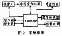
2 Visual reversing radar system constitutes a visual reversing radar consisting of most of the video rear view system and the ultrasonic ranging system. The video rear view system is responsible for collecting and displaying the rear video image, which is mainly used to replace the function of the traditional car rearview mirror. At the same time, the system is also used to display the tail end of the ultrasonic ranging system to the obstacle. Distance value. The ultrasonic ranging system is controlled by the single-chip microcomputer to complete the ranging of the obstacles behind the vehicle, and the display operation of the ranging value on the monitor is completed. Figure 2 shows the block diagram of the visual parking sensor system, in which the character stacking circuit is the MAX74560.
2.1 Ultrasonic Ranging Principle Considering the complex environment of the car, the short measuring distance and cost limitation of the auxiliary reversing system, most of the reversing radars use ultrasonic waves for distance measurement. The basic principle is to use the single-chip microcomputer to control the ultrasonic probe to emit a series of ultrasonic pulses to the rear of the vehicle, and then measure the time t after the pulse encounters the obstacle, and when the known sound wave propagates in the air v, according to the formula: ![]()
The distance between the tail and the obstacle can be calculated. Generally, the propagation speed of sound waves in the air is greatly affected by the temperature, so it is necessary to measure the air temperature and then according to the formula of the propagation speed of sound waves in the air: ![]()
Make corrections to get a more accurate distance value. In the MCU control system, because of the relationship between the operation speed and the measurement accuracy, the approximate expression of the formula (2) is often used. ![]()
Perform the calculation so that the distance measurement formula of the ultrasonic reversing radar is obtained: ![]()
From this formula, the distance from the tail to the obstacle can be calculated.
2.2 Ranging circuit According to the working characteristics of the on-board ultrasonic radar and the requirements of the working environment, the ultrasonic ranging circuit must follow the following principles when designing: 1) Considering the harsh environment of the vehicle and the convenient wiring, the ultrasonic probe must be fully sealed and waterproof. Anti-vibration type transceiver dual-purpose special probe; 2) Ultrasonic probe usually uses piezoelectric ceramic material, its resonant frequency is 40 kHz, and it has a certain inertia when starting, so it can't be driven by single pulse, 10~20 group pulse must be used The driver can achieve better results; 3) Since the ultrasonic wave propagates along a straight line, the detection range of a single probe is limited, and usually requires 3 to 4 probes to completely cover the tail. The ultrasonic distance measuring circuit designed according to the above principle is shown in Fig. 3.
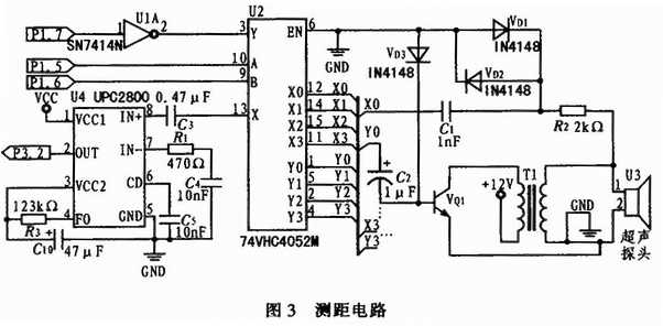
The ranging circuit is divided into two parts: transmitting and receiving. The transmitting part is driven by the SN7414 and the Y channel of the analog electronic switch HC4052 to drive four ultrasonic probes (only one of which is shown in Fig. 3). The ultrasonic probe U3 adopts a fully sealed waterproof and anti-vibration type transmitting and receiving probe for the vehicle, and the working voltage of the probe is about 120 V. In order to make it work properly, a driver consisting of VQ1, T1, C2 and VD3 is designed. VQ1 operates in the switching state. T1 is a step-up transformer with a ratio of 1:10. It is used to boost the driving voltage of 12 V to 120 V. VD3 provides a discharge path for C2. In order to prevent the high voltage when transmitting ultrasonic waves from returning through the receiving circuit C1, the HC4052 analog electronic switch is burned, and the protection circuit composed of R2, VD1 and VD2 is connected to the input end of the receiving circuit, and the signal of the input C4052 is clamped at 0. .7 V. Since the normal echo signal received by the ultrasonic probe is usually only a few tens of millivolts, the protection circuit has no effect on the echo signal.
The ultrasonic measurement adopts the cyclic working mode. The selection of the four-way probe is completed by the single-chip microcomputer controlling the HC4052 through the P1.5 and P1.6 pins. When the ranging is controlled by the internal counter of the single-chip microcomputer, 12 frequencies are generated at 40 kHz, and the duty ratio is A 50% pulse signal, sent from the P1.7 pin, is sent through the transmit circuit to the selected ultrasonic probe.
The receiving circuit consists of the X channel of the ultrasonic probe U3, HC4052 and the UPC2800. The UPC2800 is an infrared receiver-specific IC that integrates a preamplifier, an ABLC controller, a limiting amplifier, a bandpass filter, a detector, and an output shaping circuit. The center frequency of the bandpass filter can be adjusted between 30 and 80 kHz, which covers the ultrasonic application frequency of 40 kHz. Therefore, it is used in this circuit to amplify, shape and detect the echo signal. The 8 pin of the UPC2800 is the signal input pin. The 7-pin is the preamplifier gain adjustment pin. The external resistor can be adjusted between 0 and 1kΩ according to the gain requirement. The serially connected 0.1μF capacitor is used for blocking. The 3-pin is the internal power supply filter capacitor access pin. The typical value is 47μF; the 4 pin is the internal bandpass filter center frequency adjustment pin. When the external resistance value is 123 kΩ, the center frequency of the filter is 40kHz; the 6 pin is the filter filter capacitor connection terminal, and the external filter The typical value of the capacitor is O. 1μF. After the detection is completed, the pulse signal is output by the 2 pin, and P3.2 of the MCU is used as the interrupt control signal.
2.3 Video superposition and system control circuit Video superposition and control circuit As shown in Figure 4, the video signal captured by the rear camera is input through the VIN terminal of the video input terminal P1 and MAX7456 to prevent the influence of the input signal on the internal circuit of the MAX7456. Must be connected between P1 and VIN port. A 1μF input-coupling capacitor isolates the input signal from DC. The input video signal is clamped inside the MAX7456, noise is eliminated, and the character dot matrix signal is inserted. After the voltage attenuation is corrected, the VOUT terminal is output through P2 to complete the character superimposition work. The output circuit also needs to be connected to the output coupling capacitor for blocking. In order not to affect the passage of the field sync signal, the capacitor should normally take more than 330 μF. To reduce the cost and volume of the coupling capacitor, the MAX7456 connects the voltage attenuation correction capacitor to the VOUT output through the SAG port. The end is used to minimize the capacity of the output capacitor within an acceptable distortion range, as shown in Figure 4 for its typical value.
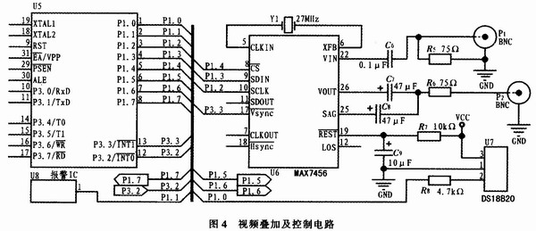
In this design, the AT89C52 is used to control the MAX7456. Since the AT89C52 does not have an SPI serial port, the MAX7456 is controlled by the timing of the P1.2, P1.3, and P1.4 ports to simulate the SPI. In order to prevent the display characters from being unstable during operation, the field sync signal output by the MAX7456 is used here. ![]() As an interrupt signal, the AT89C52 is controlled to update the data during the field blanking of the video signal to obtain a good display effect.
As an interrupt signal, the AT89C52 is controlled to update the data during the field blanking of the video signal to obtain a good display effect.
Another task of the AT89C52 is to control the ranging circuit for ultrasonic ranging. Since the distance measuring circuit has a total of 4 probes, it uses the method of cyclic ranging. The distance measuring radar is designed to measure a distance of up to 5 m. According to the propagation speed of the ultrasonic wave in the air (3), the parking radar can be calculated at 25 The sound velocity at °C is 346.45 m, which is calculated based on this. The time required for one ranging is 28.8 ms. Considering the data processing and display control time, the switching time for selecting the cyclic ranging is 40 ms. When measuring distance, it is controlled by AT89C52 internal timer. Every 40 ms, the probe is switched by the AC89C52 P1.5 and P1.6 to control the HC4052. Then, the P1.7 sends 12 frequencies of 40 kHz and the duty ratio is 50%. The pulse signal passes through the transmitting circuit to the ultrasonic probe, and the internal timer is turned on for time measurement. Since the ultrasonic probe has a residual vibration after the detection signal is transmitted, no useful signal can be detected during this period. In order to prevent the AT89C52 from being accidentally interrupted by the ultrasonic residual signal at this time through the receiving circuit, the receiving interrupt INT0 must be turned off during this period. According to the actual measurement, the ultrasonic probe used has a residual vibration of 1.7 ms at 25 °C, so the off-interruption time is set to 2 ms, and the resulting measurement dead zone is 0.35 m at 25 °C. It can be obtained from the above analysis that the measurement range of the ultrasonic radar is between 0.35 and 5 m at 25 °C.
3 The software design system program adopts modular design and consists of main program, rear view system control, temperature measurement, distance measurement, alarm, temperature and distance display. Figure 5 is the main program flow chart.
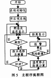
After the system is powered on, first initialize the MAX7456 and DS18B20, then turn on the camera and monitor as a video rearview mirror during driving. During this period, the MCU controls the DS18 B20 to measure the outside temperature, and sends the measured value to the MAX7456 and the camera's rear video image for superimposition and sends it to the monitor. When the MCU detects the reverse gear, it turns on four ultrasonic probes to measure the obstacle behind the vehicle, and calculates the distance from the tail to the obstacle through the detected echo time and the outside temperature. If the value is judged, it is less than the safety distance. If yes, the alarm is turned on, and the distance value is sent to the MAX7456 and the video is superimposed and sent to the monitor for display. If it is detected that the vehicle gear position is not in the reverse gear position, the distance measurement program is automatically exited and the state of the rear view mirror is restored.
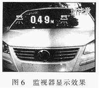
4 Test results After the actual loading test, in the environment of 25 ° C, the rough surface obstacle with a rear area of ​​1 m2, the measurement range is O. 36 ~ 5.12m. Within 3m, the measurement error is between 1.5% and 3%. When the measurement error is greater than 3 m, the error increases gradually with the increase of the measurement distance: the error is 4.6% at 5m. The display effect of the measured distance value on the monitor is as shown in Fig. 6. The field of view is clear and the prompt characters are conspicuous.
5 Conclusion Through reasonable hardware and software design, the device realizes the composite function of the reversing radar and the video rearview mirror. Compared with the traditional reversing radar, the system superimposes the radar ranging information on the image of the video rearview mirror, which conforms to the driver's visual habits, reduces the driver's working intensity, and prevents the traditional reversing radar from leaking obstacles. The report played a good role in prevention. The device has simple circuit, rich functions, low price and high promotion value.
inductors required by power supply circuits of multifunctional and small mobile phones must be small in size and low in height. These products must exhibit performance that is commensurate with the high power conversion efficiency of power supply circuits. Toroidal Ferrite Core Choke Coil inductor,Power supply circuits must also exhibit resistance to noise in the power supply state. All performance requirements of this component is expected based on the wire-wound inductors
Packaging Details
Packaging details:
Plastic packing bags inside, Carton box outside
Detail is according to the requirement of customer
Delivery Detail:
5-10 Days after received the order payment.
Delivery Time
15days

Toroid Core Inductor, High Current Toroid Choke Coil, Toroidal Ferrite Core Choke Coil, Magnet Coil Choke Inductor
JINAN EMI SHIELDING TECHNOLOGY CO., LTD. , http://www.emirfi.com