1 Introduction
Wearable medical instruments enable non-invasive, non-invasive medical monitoring of the human body, with features such as mobile operation, ease of use, and long-term continuous operation. It can reduce the physiological and psychological burden of the patient and achieve better detection results. Therefore, its development has received more and more attention. At present, the wireless transmission means for the wearable medical instrument to realize the monitoring instrument from the human body to the upper computer of the user terminal include Bluetooth, radio frequency, infrared and the like. From the existing literature, Bluetooth is the most widely used. However, the high cost of Bluetooth is a big obstacle to the future of the instrument. The infrared transmission distance is short and the anti-interference is poor, and it is basically not used now. RF has the characteristics of low price and long transmission distance, especially the emergence of cost-effective RF chips, making its use more and more popular. This paper designs a radio frequency chip based on nRF905 to realize the wireless transmission of physiological signals. At the same time, compared with other similar designs, the design also fully considers the security of the user's physiological information, and encrypts the data before the data is transmitted wirelessly to protect the user's health and privacy.
2 system structure design
The overall structure of the design consists of physiological signal acquisition circuit, data encryption, RF transmission, reception and several modules of the user host, as shown in Figure 1. First, the physiological data to be monitored is acquired by the acquisition circuit; then the acquired data is encrypted and then sent to the host through the radio; the host performs subsequent processing on the received data. The front end and the back end can communicate with each other via radio frequency.
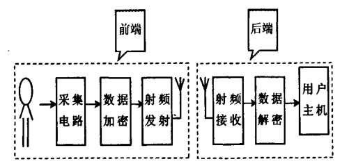
Figure 1 overall design block diagram
2.1 acquisition circuit
The acquisition circuit is mainly composed of a sensor circuit, an amplification filter circuit and an A/D conversion.
(1) Sensor circuit: The sensor converts the physiological signal to be monitored into an electrical signal, and different sensors are required to monitor different physiological signals. In this design, the main electrocardiogram and pulse wave are monitored. The sensors used are patch electrodes and infrared photoelectric sensors. The ECG detection uses a three-lead method.
(2) Amplification filter circuit: The bioelectric signal obtained after the sensor conversion has a low amplitude and a large noise interference, and must be amplified and filtered. The amplification factor of the amplifying circuit needs to comprehensively consider the magnitude of the physiological signal acquired by the sensor and the dynamic range of the A/D converter. In this design, the magnification of the electrocardiogram and pulse wave are 1000 times. The filtering process includes bandpass filtering and 50 waves. In the design, the band-pass filtering uses a second-order active band-pass filter circuit, and the bandwidth corresponding to the electrocardiogram and the pulse wave are 0.1 Hz-1 and 0.1 Hz-30Hz, respectively. 50Hz power frequency interference is the source of noise of physiological signals, and the effect of 50Hz interference cancellation directly determines the quality of the most acquired signals. This design uses an asymmetric RC network trap, which has the advantage of adjusting the notch frequency and Q value according to the interference source frequency and interference intensity.
(3) A/D conversion: The 10-bit A converter is used in the design. The dynamic range is -2.7V to 2.7V, the sampling of the electrocardiogram is 200Hz, and the sampling frequency of the pulse wave is 60Hz. Since the design of the above circuits is currently quite mature, the specific design of these circuits will not be described in detail herein.
2.2 Data encryption and decryption
This design uses nRF905 RF chip to achieve data non-shooting and receiving, any same chip, as long as the internal registers are consistent, they can achieve data communication. Since the user's physiological signal involves the user's privacy problem, J, in order to ensure the security of the user data during wireless transmission, the data must be encrypted, and this step is often ignored in similar research [3]. J. In this design, the AES∞o (Advanced EncrypStandard) software encryption algorithm is used to complete this process. Commonly used hardware encryption, on the one hand, improves the portability of the instrument, on the other hand, it can reduce the cost of the instrument. AES algorithm is a method of packet encryption, which is divided into two methods of encryption and decryption.
section. It converts a certain length of plaintext packets into corresponding rounds. Each time the key is transformed from a certain length of initial key, and finally the encrypted ciphertext packet is obtained, and the length is the same as the plaintext packet. When decrypting, the ciphertext is grouped into the inverse transform of the same number of times, and the inverse transform is the inverse process of the round transform, thereby obtaining the original plaintext packet.
AES supports 128, 192 or 256-bit three-layer design with a 128-bit key length.
2.3 RF transmission and reception
This design uses nRF905 RF chip to achieve data transmission. The nRF905 is a transmitter chip from Nordic, Norway. The 32-pin QFN package (5&TImes; 5mm) is 1.9V to 3.6V and operates on the 433/868/ISM channel (free of charge). nRF905 can handle the work of header and CRT (Cyclic Redundancy Check), can automatically complete Manchester encoding/decoding by on-chip hardware, communicate with microcontroller using SPI interface, configuration is very convenient, its power consumption is very low, with one The output power of 10dBm is only 1m when the current is only 11m in the receiving mode. The nRF905 not only requires low power consumption for medical devices, but also guarantees both transmission rate and transmission distance. According to the actual measurement, there is a wall block in the room, and in the case of no strenuous exercise, the transmission distance reaches 30m or more, so the monitored person can move freely indoors. The wireless transmission loss rate is within 1/10 000, which ensures that the transmission data is not lost. The maximum transmission rate is up to 100kbs.
2.3.1 Hardware Connection
In the design, the front end adopts C8051F330 single-chip microcomputer (MC now controls nRF905, and the back end adopts s3C2440 (ARM9) to control. Its structural block diagram is shown in Figure 2:
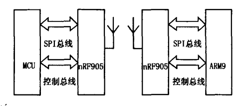
Figure 2 signal transceiver circuit block diagram
MCU and ARM9 configure the nRF9 registers through the SPI bus, mainly to configure five types of registers: one is the RF configuration register for a total of 10 bytes, including the center frequency, wireless transmit power configuration, receive sensitivity, and send and receive data. The number of valid bytes, receiving address configuration and other important information; the second is to send data registers, a total of 32 bytes, the MCU to send out the data needs to be written here; the third is the sending address, a total of 4 bytes, a pair of transceiver For the device to communicate normally, the sending address of the transmitting end needs to be the same as the receiving address of the receiving end; the fourth is the receiving data register, which is 32 bytes in total, and the valid data received by nRF905 is stored in these registers, and the MCU can come here when needed. Read; five is the status register, 1 byte, contains address matching and data ready information, generally not used. The control bus is mainly used to select different working modes of nRF905 (four modes, as shown in Table 1); query the current status of nRF905 (whether data transmission or reception is completed); enable SPI of nRF905.
Table 1 nRF905 work 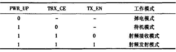
2.3.2 Software Design
The front end of this design uses the C8051F330 microcontroller for real A/D conversion and control of nRF905. C80 has a 10-bit A/D converter, supports SPI communication, low volume power consumption and fast operation, so it has a wide range of applications. The front-end software design flow chart 3 of this design is shown as follows: First, the MCU is initialized, including the settings of the A/D converter and the SPI communication mode. The MCU then configures the five registers of the nRF9 via the SPI bus as needed. After the initialization is completed, the MCU queries whether the backend requests the number to be sent. When the backend has a request to send a number (a specific command word is sent to the front end through the nRF905), the MCU starts the A/D conversion, then encrypts the converted number and sends it to the backend through the nRF905. The software design flow of the back end is similar to the front end point. First, the ARM9 and nRF905 are initialized. Then, the nRF905 sends a request for sending a number to the front end, then receives the data, decrypts the received data, and finally further processes the decrypted data. . In particular, when configuring the nRF905 sending address at the front and rear end, note that the sending address of the sending end should be the same as the receiving address of the receiving end device. In actual work, nRF90 can automatically filter out data with different addresses, only the address matches and the school The correct data is accepted and stored in the Receive Data Register.
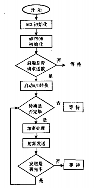
Figure 3 software design process
3 Experimental results
In the experiment, in order to avoid the conflict between the time requirement of AES encryption and the A/D sampling rate, the execution efficiency on the 128-bit AES encryption C8051F330 was first calculated, and it was found that the time required to complete the secret was about 3.8ms. . This has no time conflict with the design center power and pulse wave sampling rates (5ms and 16.7 Peng, respectively). The back end uses the S3C2440, which performs much faster than the C80, so time is guaranteed to be free of conflicts. At the end of the experiment, the ECG and pulse wave were monitored separately, and the data received by the back end was displayed on the PC sent by the serial port. The display program was written in VC6.0, and the results are shown in Figure 4 and Figure 5. :
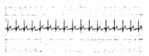
Figure 4 Received ECG signals 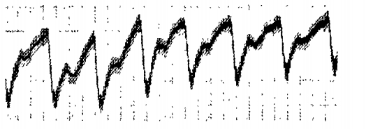
Figure 5 Received pulse signal
4 Summary
This design uses the nRD05 radio frequency chip to realize the wireless transmission of physiological signals from the human body to the user host in the wearable medical device. At the same time, the design fully considers the security of data transmission, and performs 128 AES encryption processing on the data. It can be seen from the experimental results that the design can prove the real-time, safe and accurate wireless transmission of physiological signals. At the same time, it can be seen that since the front-end control chip uses an MCU, its processing speed is limited. Therefore, if you want to monitor physiological signals with a higher frequency range (such as heart sound: 3Hz - S00H2) or monitor multiple physiological parameters at the same time, use a higher processing speed chip, such as DSP. In addition, the design of the back end is ARM9, its processing speed, coordination performance are particularly strong, you can add some hardware devices, such as LCD, the back end as a handheld device, or add some remote transmission hardware such as GPRS, The signal is transmitted remotely, which greatly enhances the function of the instrument. These are also the work we will start further in the future.
HQQN wholesale all model li-polymer Iphone Battery from iphone 4 battery to Iphone X Battery. This battery is 1510 mAh pure cobalt li-po battery for iphone 5C, Quality and size same as original IPhone 5C Battery. the standby time is about 100 hour, 4 G Internet Time is about 10 hour and call time is about 7 hour. All battery we have FCC, ROHS, FCC certifications. We supply OEM & ODM service more than 7 years, expecting working with more customer in future.

Iphone 5C Battery ,5C Battery,Apple 5C Battery,Apple Iphone 5C Battery
Shenzhen Hequanqingnuo Electronic Technology Co., Ltd. , https://www.hqqnbattery.com