The most important feature of organic light-emitting diodes (OLEDs) is that they are self-illuminators, do not require backlights and color filters, and are thinner than LCDs. In addition, they have a wider viewing angle range, faster response speed, and lower The driving voltage, color and contrast ratio are also higher than LCD. In theory, it can achieve lower consumption and simple design. It is a widely recognized display star after LCD. Although Oled has so many advantages, its lifetime is shorter than that of LCDs, because OLEDs are current-driven self-illuminators with relatively short material and component life.
OLED power supply specifications
Generally, a small-sized OLED requires a set of positive voltage (Vdd) and a set of negative voltage (Vss) to supply power. The power architecture can be divided into two types: digital camera and mobile phone architecture. Digital camera power supply specifications are: Vdd voltage range is 3V to 6V, Vss voltage range is -7V to -10V; mobile phone power supply specifications are: Vdd voltage is about 2.5V, Vss voltage range is -7V to -10V. The input power for these two products is usually a lithium battery with a voltage range of approximately 3V to 4.2V.
Digital Camera Vdd Solution
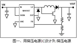
Since the Vdd voltage range is 3V to 6V, the Vdd power architecture should be Buck/Boost or Boost. If we can't find the power of the Buck/Boost architecture at the moment, we can also use the very popular Buck architecture to design it into a Buck/Boost architecture, using a common set of buck power control ICs, plus a MOSFET and an output diode. , can be designed as Buck / Boost output, as shown in Figure 1. The regulator works by increasing the inductor current by the slope of Vin/L when Lx is high, and decreasing the slope of (Vout+VD)/L when Lx is low. The input and output currents are intermittent and allow the output voltage to be higher or lower than the input voltage.
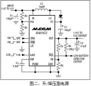
Designers can also use a set of Buck/Boost power ICs to generate the required voltage output. Figure 2 shows a set of direct up/down conversion ICs. It combines a set of boost converters and linear regulators to provide a conversion scheme that can both boost and step down. This converter provides a stable output when the input voltage is higher or lower than the output voltage. The input range is 1.8V to 11V. It can be preset to 3.3V or 5V output. It can also be obtained by using two voltage divider resistors. Adjusted output voltage: 1.25V to 5.5V, efficiency up to 85%. If an output between 3.5V and 4V is required, it can be implemented by a combination of a boost converter and a linear regulator. Such as: MAX1606 boost converter and MAX8512 linear regulator combination.
From the perspective of cost reduction, the charge pump can be selected without inductors and output diodes. For example, the MAX1759 charge pump uses a step-up/step-down configuration to produce a stable output. Despite its operating frequency above 1.5MHz, it can maintain quiescent currents as low as 50uA.
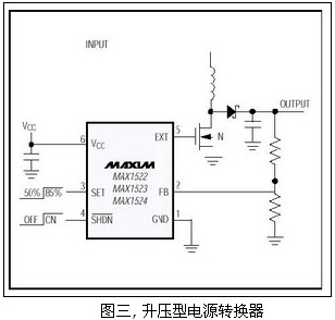
In order to pursue higher conversion efficiency, some designers choose the boost mode to generate a set of stable outputs higher than the input, as shown in the boost architecture of Figure 3. Since the power switching MOSFET is external, it provides a large output power. A boost converter with a built-in MOSFET power switch, such as the MAX1722, can also be selected to save space and reduce cost, depending on the output power.