0 Preface
Semiconductor power devices have generally undergone three stages by material. The first generation of semiconductor power devices is mainly represented by Si bipolar power transistors, and is mainly used in the S band and below. The Si bipolar power transistor can achieve hundreds of watts of output power in the L-band and nearly 200W in the S-band. The second-generation semiconductor power devices are represented by GaAs field-effect transistors, and their maximum operating frequency can reach 30-100 GHz. GaAs FETs have a maximum output power of nearly 100W in the C-band and 25W in the X-band. The third generation semiconductor power devices are mainly represented by SiC field effect transistors and GaN high electron mobility transistors. Compared with the first and second generation semiconductor materials, SiC and GaN semiconductor materials have the advantages of wide band gap, high breakdown field strength, high saturation electron drift rate and strong radiation resistance, especially suitable for high frequency and high. Power, radiation-resistant power devices, and can operate in harsh environments with high temperatures. Due to these advantages, wide bandgap semiconductor power devices can significantly improve the performance of electronic information systems, and are widely used in important fields such as satellites, rockets, radars, communications, fighters, and marine exploration.
This paper designs and implements an efficient GaN wide bandgap power amplifier based on Agilent ADS simulation software. The design steps are detailed and the amplifier is tested. The results show that the amplifier can achieve more than 15W in power from 2.3 to 2.4 GHz. More than 67% of the output.
1 GaN wide bandgap power amplifier design
1.1 Amplifier design specifications In the 2.3 to 2.4 GHz operating frequency band, the amplifier is required to operate in continuous wave with an output power greater than 10 W and an additional efficiency exceeding 60%.
1.2 Selection of power tube According to the design specifications required by the amplifier, the SiC-based GaN wide-bandgap power tube provided by an import company is designed and selected. The main performance parameters are shown in Table 1.
This article refers to the address: http://
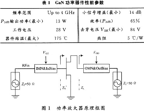
1.3 Amplifier Circuit Design Figure 1 is a block diagram of the power amplifier. In Figure 1, IMN&Bias and OMN&Bias are the input matching network and the input bias circuit and the output matching network and the bias circuit. VGS and VDS are the gate-source operating voltage and the drain-source operating voltage, respectively. The design idea adopted is: DC analysis of the power tube to determine the static working voltage of the amplifier; stability analysis and design; source pull and load pull methods to determine the optimal source impedance of the power tube matching circuit ZS and optimal load impedance ZL (ZS and ZL are defined in Figure 1);
Input and output matching circuit design and bias circuit design according to the obtained source impedance and load impedance; processing, debugging and revision.
1.3.1 DC Analysis The purpose of DC analysis of a power amplifier is to determine the static operating voltage of the power tube through the current-voltage (IV) curve of the power tube. Since the manufacturer provides the ADS model of the power tube, the simulation design is directly used in the design (the same below).
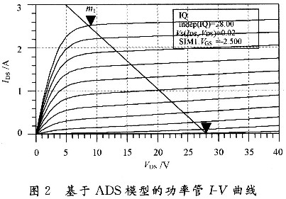
Figure 2 shows the results of a DC analysis of the device model in the Agilent ADS software. According to the device specification parameters given by the manufacturer and the IV curve in Fig. 2, VDS=28 V and VGS=-2.5 V are selected as the operating voltage of the amplifier. In order to achieve higher efficiency of the amplifier, the static voltage is chosen here to make the amplifier work under Class C conditions.
1.3.2 Stability Analysis Stability is one of the key factors to consider in the design of an amplifier. It depends on the S-parameter and termination conditions of the transistor. The instability of the power amplifier will produce undesirable parasitic oscillations, resulting in distortion of the results and even design failure. Therefore, stability analysis and design must be performed before the amplifier impedance matching circuit is designed.
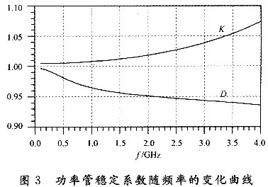
Figure 3 shows the power tube stability factor as a function of frequency. In Figure 3, the stability coefficients K and D are defined as: 
It can be seen from Fig. 3 that the stability coefficients K and D satisfy the conditions of greater than 1 and less than 1, respectively, in the design frequency band, so the power tube is unconditionally stable.
1.3.3 Source Traction and Load Traction Analysis Source Traction/Load Traction Analysis Method Principle: The amplifier analyzes the power tube by continuously changing the source impedance/load impedance under large signal level excitation, and then on the Smith impedance chart. Draw the equal power curve and the equal gain curve, and select the best source impedance/optimal load impedance according to the design requirements to accurately design the power amplifier that meets the requirements.
In the analysis, the center frequency f = 2.35 GHz was selected. In order to accurately obtain the optimal source impedance ZS and the optimal output impedance ZL of the power tube, the efficiency priority strategy is followed in the analysis process, and the following steps are taken:
First, assume ZS(O)=10 Ω for load traction analysis to obtain ZL(1); then, obtain ZS(1) by source traction analysis according to ZL(1); then obtain ZL by load traction analysis according to ZS(1) 2),…. The source traction analysis and the load pull analysis are repeated until the load impedance ZL obtained twice before or after is equal or the phase difference is small.
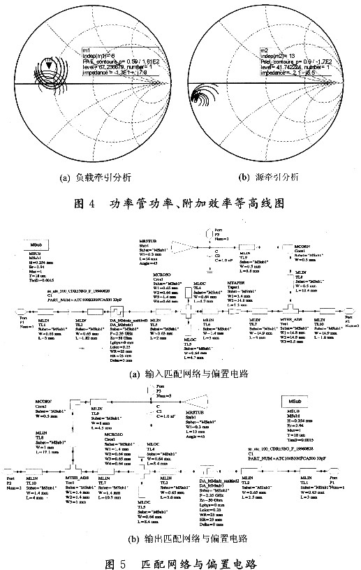
Figure 4 is a power line output power, Power Added Efficiency (PAE) contour map obtained by source traction analysis and load traction analysis. In Figure 4, the additional efficiency of the power tube is defined as: ![]()
Where: POUT, PIN and PDC are the amplifier output power, input power and power consumption, respectively; ηPAE stands for power added efficiency.
From Fig. 4, it can be seen that the optimum source impedance and the optimum load impedance of the power amplifier are ZS = 2.1 - j6.5 Ω and ZL = 13 + j7.8 Ω, respectively.
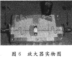
1.3.4 Matching Network, Bias Circuit Design The matching circuit is mainly used for impedance transformation. The ultimate purpose is to achieve maximum power transmission. In the simulation design process, it is first assumed that the input and output matching network design is performed using the optimal source impedance and the optimal load impedance in the case of an ideal bias circuit, and then the bias circuit design is performed according to the 1/4λ criterion, and The bias circuit satisfies the requirements of RF turbulence by fine-tuning the parameters of the circuit. In the Agilent ADS software, in order for the design to accurately simulate the real situation, RFMomen-tum optimized simulation is generally required after the circuit design (model-based). Figure 5 shows the amplifier matching network and bias circuit designed by Agilent ADS software. In Figure 5, the microwave circuit substrate material is selected from Rogers' RT/duroid 6002 sheet, the dielectric constant is 2.94, and the thickness is O. 254 mm. During the optimization simulation, it was found that the efficiency and bandwidth of the amplifier are a contradiction. When the efficiency is improved, the bandwidth is narrowed, and vice versa.
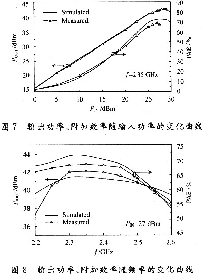
2 indicator test amplifier physical object shown in Figure 6.
A wide bandgap power amplifier was designed for testing. The test conditions are: continuous wave operation, drain voltage VDS = 28 V, and gate voltage VGS = -2.5 V. Figure 7 shows the output power and additional efficiency of the amplifier as a function of input power at a frequency of 2.35 GHz. The test results show that as the input power increases, the output power of the amplifier increases approximately linearly, and saturation begins to appear at 26 dBm. As the input power increases, the additional efficiency of the amplifier increases, reaching a maximum at 27 dBm. The additional efficiency is 68.5%. The experiment also tested the amplifier's output power and additional efficiency parameters in the 2.2 to 2.6 GHz frequency range (0.5 GHz step size). The test results are shown in Figure 8. In the frequency range of 2.25 to 2.5 GHz, the amplifier output power is above 10 W, and the additional efficiency is also over 60%. In the frequency range of 2.3 to 2.4 GHz, the output power exceeds 15 W, and the additional efficiency exceeds 67 9/6. The amplifier meets the design specifications.
3 Conclusion The S-band 10 W power amplifier was designed and fabricated using SiC-based GaN wide bandgap power devices. The test results show that the designed amplifier has an additional efficiency of 67 9/6 or more in 2.3 to 2.4 GHz, which also proves the high efficiency and high gain of the wide bandgap device.
XXR offers Heat Shrinkable sleeves with RSBA series, RSBJ series, RSB series, RSY series, RSBAD series and SBZS series.
1. High performance heat shrinkable closure for unpressurized applications or air-blorcking pressurized cable networs.
2. Able to work under an environment of -30 degrees centigradeto +90 degrees centigrade for a long term
3. Suitable for aerial, buried applications
4. It is of super composite fiber structure and secondary sealing, featured by high mechanical strength, strong tearresistant, and strong shrinkage and excellent resistance to weathering.
5. Super heat shrinkable sleeve sealing gel material is composed of several layers of specially blended polymers, adhesives and fiber-reinforcing layer. The fiber-reinforcing layer provides excellent mechanical strength and eliminates the propagation of localized damage that can result from overheating or other errors in installation. Once the closure sleeve has been installed, the composite design of the Super Sleeve sealing gel material provides superior mechanical protection from forces such as impact, abrasion, UV light, and atmospheric contamination
6. The heat shrinkable closure bears excellent leakproofing, moisture-resistance and pressure-containing capacity; The softening point can be up to 130 degrees centigrade, suitable for the area of high ambient temperature.
7. Range of closures to suit all cable sizes
8. Simple and easy to install
Heat Shrinkable Sleeves For Copper Cable
Heat Shrinkable Tubing ,Heat Shrink Wrap Tubing,Heat Shrink Tubing
Chengdu XingXingRong Communication Technology Co.,Ltd , http://www.xxrtx.net