1 Introduction
With the acceleration of urban modernization construction, the society has higher requirements for urban road lighting and urban lighting projects. The state clearly requires that resources be saved as the country's basic national policy, and energy conservation has become the mainstream of social development.
This paper designs a hardware platform based on ATmega128 processor and designs a PWM chopper voltage regulator circuit to achieve reasonable adjustment of street lamp voltage. The voltage automatic adjustment circuit is mainly based on the PWM chopping technology, and the actual circuit is designed. The debugging is successful and the purpose of the buck is achieved. In view of the high operating frequency of the switching tube in this kind of step-down circuit, high-order harmonics are generated. In order to suppress higher harmonics, the filtering circuit is designed through specific calculation, and the debugging is successful.
2 overall system design
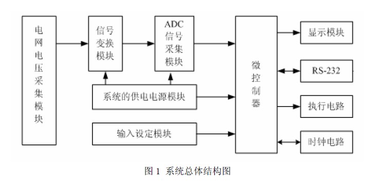
As shown in Figure 1: Firstly, an AC voltage regulation system is established. The controlled object of the system is the grid voltage. The controller chops the grid voltage waveform by AC chopping technology to achieve the voltage regulation effect and collects voltage. The circuit collects the output voltage, the controller obtains the sampled value of the voltage and analyzes it, and performs the next adjustment on the controlled object according to the analysis result until the output voltage reaches the ideal state; secondly, the design of the communication interface, RS- 232 serial communication function to transmit data interface circuit design, form a complete communication function; again, the system's versatility, interactivity and user-friendly design, through the keyboard interface to set system parameters, and through the liquid crystal display module display operation Requirements and data.
3 system hardware circuit design
3.1 Pulse width modulation step-down design ideas
The method mainly controls the frequency of the switch to reduce the effective value of the output voltage to achieve the purpose of voltage reduction. The frequency of the PWM is 180KHz-200KHz, which can be steplessly adjusted, and the output voltage waveform is a standard sine wave, but filtering is required.
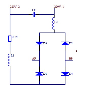
Figure 2 Pulse width modulation step-down schematic
As shown in the circuit of Figure 2, in the bridge rectifier circuit consisting of diodes D1, D2, D3, and D4, due to the unidirectional conductivity of the diode, it can be judged that the voltage at point A is always higher than the voltage at point B. The triode is connected between A and B, and the output of the bridge circuit is controlled by the switching characteristics of the triode. This is the so-called pulse width modulation principle. When the control voltage is a series of pulses of equal amplitude and unequal width, and the pulse width is modulated according to a certain rule, the corresponding output voltage can be obtained. At this time, the waveform outputted by the circuit is the voltage waveform after being cut by the high-frequency pulse. In order to obtain a standard sine wave and reduce the influence of the high-frequency component on the power quality, a reactor is connected in series at the input and output ends of the circuit for leveling. wave. In summary, a circuit that uses the pulse width modulation principle to change the output voltage by controlling the rectifier circuit is obtained. Although the waveform generated after passing through the circuit has harmonics and needs filtering, its cost is relatively low, and the output is a standard positive harmonic.
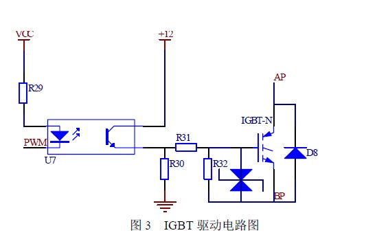
Pay attention to the following points when designing the drive circuit of the IGBT:
(1) The IGBT gate-level withstand voltage is generally around ±20V. Therefore, the output of the driver circuit should be provided with a gate over-voltage protection circuit. The usual practice is to connect a Zener diode or a resistor in parallel with the gate. The drawback of the shunt regulator diode is that it will increase the equivalent input capacitance inC, thus affecting the switching speed; the defect of the shunt resistor is to reduce the input impedance and increase the drive current. The latter is chosen in this paper.
(2) Although the power required for driving the IGBT is small, since the input capacitance inC of the MOSFET exists, the capacitor needs to be charged and discharged during the switching process, so the output current of the driving circuit should be sufficiently large, assuming that the driving is turned on, within the rising time rt To linearly charge the input capacitance inC of the MOSFET, the drive current is GEinGSrI=CUt, where 2.2rint=RC can be taken, where R is the input loop resistance.
(3) In order to reliably turn off the IGBT and prevent the lock-up effect from occurring, a negative voltage is applied to the gate, so the dual-supply should be used to supply power to the drive circuit. The specific drive circuit diagram is shown in Figure 3.
3.2 Signal sampling circuit design
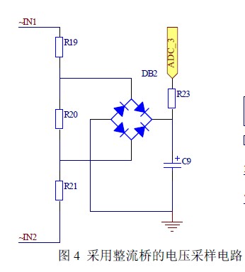
The real-time acquisition of grid voltage and current signals and the accuracy of their sampling determine the performance of the system to a large extent. According to the analysis of the integrated ADC performance of the Atmega128 microcontroller, the main technical indicators such as conversion time, resolution, linearity error, range and reference voltage are considered, and it can be judged to meet the requirements of system design, and through external precision reference. The way the power is supplied to ensure the accuracy of the system. For the front-end signal conversion module for grid signal acquisition, we mainly consider several factors: First, the quality of the sampled signal can not only reflect the voltage and current of the grid, but also cause interference to the system. This requires good circuit. The isolation measure; the voltage range of the next sampled signal is consistent with the range of the reference voltage of the ADC, and the design exceeding or below the working range of the reference voltage is unreasonable; third, attention should be paid to the impedance matching problem, if the impedance is not Matching, the resulting sample values ​​do not accurately reflect the parameters of the grid signal and may burn the input port of the ADC.
Since the AD sampling port of the MCU can only sample a positive voltage, the AC voltage to be sampled is stepped down by the transformer, rectified and divided, and then sampled. At this time, the voltage is limited to 0V-5V, in order to maintain the sampling voltage. Accuracy and stability, a capacitor in parallel with the input port is anti-interference, and a resistor in series meets the requirements of ADC impedance matching. Its circuit diagram is shown in Figure 4:
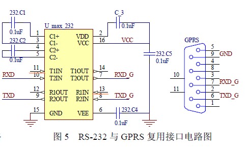
3.3 RS232 interface circuit
The simplest connection between a PC and a single-chip microcomputer is a zero-modulation three-wire economy. This is the minimum number of circuits necessary to perform full duplex communication. The PC is configured with the RS-232C standard serial interface. The electrical specifications of the two are inconsistent. Therefore, to complete the data communication between the PC and the MCU, level conversion must be performed. The chip selected for this design is MAX232, which converts the TTL level to RS. -232 level. At the same time, because RS-232C standard serial interface is widely used and mature technology, we choose RS-232C standard serial interface. The specific circuit is shown in Figure 5:
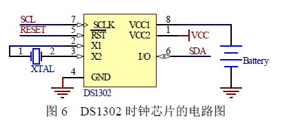
3.4 Clock chip circuit design
Dallas Semiconductor's DS1302 trickle charge clock chip is a programmable I2C serial interface clock chip. It also provides 31 bytes of nonvolatile SRAM for data storage. The structure is simple and can be used as SCL through any I/O port of the microcontroller. And SDA signal line, programming is simple, the cost is low; the disadvantage is that the power loss data is lost. The time and date of the system can be backed up with supercapacitors or rechargeable batteries if the corresponding data is stored. Its circuit is shown in Figure 6.
3.5 LCD circuit design
In the process of working in the lower position machine, the parameters of the system should be displayed in real time. For the display module, an LCD liquid crystal display is used, and its model number is CM19264. Compared with LED, it has small operating current and large display capacity, which can display Chinese characters and images. It is beautiful, generous and easy to display. In programming, the LCD has a separate controller and internal memory, and its display can be stored by the internal controller, so dynamic scanning is not required, saving system time.
3.6 Keyboard Design
System parameters are set by chain buttons. The chain button is similar to the determinant keyboard in software programming. This design uses 15 keys and shares the 6 I/O ports of the MCU. A total of 10 numeric keys, 4 direction selection keys and a confirmation key are provided to make the keyboard interface design user-friendly. Saves 2 I/O ports compared to the determinant keyboard.
3.7 Power circuit design
In the system work site, the power supply can realize on-site power take-off, transform the grid voltage through the transformer, and then convert it into DC power through the rectifier circuit, and then stabilize it at a certain voltage value to provide power for the system work through the integrated voltage regulator. Powered by ±5V and ±12V supplies. The power module can use linear three-terminal regulators 78LM05, 79LM05, 78LM12, 79LM12, 78xx series quiescent current is 5mA ~ 8Ma, in the use of heat sink to heat it, improve power efficiency, and right overload or short circuit Protection, mature technology and low cost. The ADC reference voltage uses the LM336-5.0 chip, which also ensures the ADC's range and its sampling accuracy.
4 system software design
The various modules of the aforementioned hardware circuit are the basis of the system for sampling the field voltage. The programming of the microcontroller is the core of the whole lower-level machine system, and can coordinate the efficient and accurate work of each module. The MCU program design includes six main parts: the grid voltage acquisition A/D conversion subroutine, the LCD display subroutine, the keyboard control subroutine, the digital signal processing subroutine, the control output subroutine, and the serial communication subroutine.
After the system is powered on, the internal resources of the MCU are initialized, including setting the stack pointer, prohibiting the interrupt and determining the priority, setting the working mode of each timer/counter, etc.; then initializing the external device of the MCU, including the LCD, Clock chip and serial port. After the initialization, the system starts to work. First, the grid voltage is sampled, and calculation is performed. The grid voltage is controlled according to the corresponding algorithm. The keyboard and LCD display interface are queried, each set value is displayed, and the setting is performed; the time of the time chip is read in time. Value, and hierarchically regulate the grid according to different time periods. Use the interrupt method to upload data from the serial port.
5 system anti-interference measures
The system runs in a complex environment, and it is easy to run out of control, causing the program to enter an infinite loop, and even issue a wrong execution action, causing great losses. The anti-interference ability of the system largely determines the reliability of its work, so the anti-interference problem should be considered in an important position in the design process of equipment and systems. In this design, the following hardware anti-jamming measures are mainly used:
(1) Independent power supply
In order to isolate the analog circuit portion from the digital circuit portion, an independent power supply is designed to supply power to the digital circuit portion. Therefore, the digital part of the system is powered by an independent power supply, which not only further isolates the analog part and the digital part, but also suppresses spikes, overvoltages, surges, etc. caused by increased harmonics and voltage instability of the power grid. Part of the impact, thus ensuring that the detection system works properly.
(2) Grounding measures
The analog ground and digital ground connection of the system are grounded at a single point. If multi-point grounding is used, a potential difference may be generated between multiple grounding points, which in turn generates noise current, which affects the normal operation of the system.
(3) PCB wiring anti-interference
In order to ensure the correctness of signal transmission in design, when designing the signal routing of PCB, the signal line is designed according to the following principles: the trace is as short and thick as possible, and the 45° oblique line or arc is taken when turning, absolutely avoiding 90° Corner; the digital line and the analog line are separated. If it is unavoidable, the two lines are vertical; the high-current fast signal line is as close as possible to the ground line, and capacitor filtering is taken when necessary.
6 Summary
The street lamp energy-saving device is safe and reliable, prolongs the service life of the street lamp, reduces the power consumption, and produces greater economic and social benefits.
references:
[1]. ATmega128 datasheet http://
[2]. RS-232 datasheet http://
[3]. MAX232 datasheet http://
[4]. TTL datasheet http://
[5]. DS1302 datasheet http://
[6]. 78xx datasheet http://
[7]. LM336-5.0 datasheet http://
[8]. PCB datasheet http://
The Samsung S8 Plus Battery replacement have been undergo thoroughly tested,we have stricter QC inspection standards than other regular suppliers.All Samsung phone batteries built-in certified Grade A+ battery cells,CE,FCC and RoHS certified.Our Samsung S8 Plus battery replacement will provide you with up to 500 lifetime charge cycles,work as good as your original Galaxy S8 plus battery.
As a professional manufacturer over 7 years experience,we Hequanqingnuo technology owns the brand of HQQNUO involved in different kinds of Cell Phone Battery such as Iphone Battery , Huawei Battery , Samsung Battery and other Cell Phone Accessories such as iPhone Charger Case, QI Car Charger ,Wireless Phone Charger etc.

Samsung S8 Plus Battery
Samsung S8 Plus Battery,Battery For Samsung S8 Plus,Samsung Galaxy S8 Plus Battery,Battery For Samsung Galaxy S8 Plus
Shenzhen Hequanqingnuo Electronic Technology Co., Ltd. , https://www.hqqnbattery.com