Due to the continuous development of embedded system application technology, the requirements for core processor performance are getting higher and higher, and some traditional 51 series control chips are difficult to perform many complicated tasks. Therefore, through research and analysis, we have developed a set of experimental development system based on ATmega8 high-performance series single-chip microcomputer. ATMEL's ATMegs8 microcontroller is a unique 8-bit RISC CPU with on-line self-programming Flash and single-clock instructions, C-language, Basic-optimized instruction set, and rich on-chip peripheral interface circuitry. The powerful ATmegs8 microcontroller is a highly flexible and cost-effective chip that provides an excellent solution for many high-end embedded system designs.
1 overall system design
The overall design principle block diagram of the MCU multi-function experiment instrument hardware is shown in Figure l:
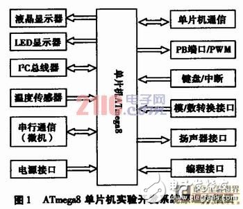
In the single-chip experimental development application system, the ATmega8 MCU core module communicates with the PC host computer through RS-232, making full use of the resources of the PC. The power part is connected to the PC by USB, and the power of the host computer is used. In addition, the experimental development system is designed with a downloader, which can be started with only one download line, without the need to purchase an expensive programmer, which is convenient to use and saves cost. The experimental system can be guaranteed to have a high cost performance.
In the experimental software, you can use either C or BASCOM-AVR programming software. BASCOM-AVR programming software provides a powerful, concise and convenient software platform for developing AVR microcontrollers. Its BASIC language is highly compatible with QB. It is easy to understand and learn. The fully functional hardware simulation platform makes the learning, experiment and development of single-chip microcomputer simple. It's easy and fun, and many designs know the results in computer simulations. With BASCOM-AVR, it is possible to popularize AVR microcontrollers on a large scale, providing excellent solutions for many high-end embedded system designs.
Collection
Comments (0)
share to
LinkedIn2 hardware circuit design
2.1 CPU module design
ATmegs8 is a new AVR high-end microcontroller introduced by ATMEL in the first quarter of 2002. ATmegs8 integrates a rich hardware interface circuit and two 8-bit timer/counters with a pre-scaler (Separate Prescale). 1 prescaler (Separat Prescale), 16-bit timer/counter with compare and capture modes, 1 asynchronous real-time clock (RTC) with independent oscillator, 3 PWM channels, can implement any 16-bit, phase And frequency adjustable PWM pulse width modulation output, 8-channel A/D conversion (TQFP, MLF package), 6 10-bit A/D+2 8-bit A/D, 6-channel A/D conversion (PDIP package) 4 channels 10 bits A/D+2 channels 8 bits A/D, 1 I2C serial interface, support master/slave, send and receive four working modes, support automatic bus arbitration, 1 programmable serial USART interface Support synchronous, asynchronous and multi-machine communication automatic address recognition, 1 SPI synchronous serial interface supporting Master/Slave, receiving/transmitting, programmable watchdog timer with on-chip RC oscillator, On-chip analog comparator. The CPU module designed around the core chip is shown in Figure 2.
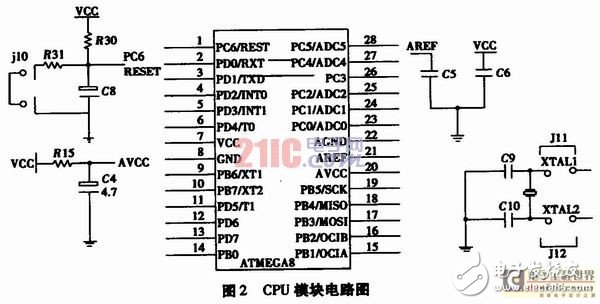
There are two options for the reset circuit RESET in the figure: external reset, J10 must be inserted into the short-circuit block; or PC6 for I/O port, J10 pull out the short-circuit block.
The crystal oscillator circuits XTAL1 and XTAL2 in the figure are the input and output terminals of the inverting amplifier of the on-chip oscillator, respectively. An external crystal oscillator is connected. The fuse position CKOPT is programmed and the range of C9 and C10 is set (12μm~ 22 μm) gives the ATmega8 a wide operating frequency range (3.O MHz to 8.0 MHz). There are two options for crystal oscillator: external 8 MHz passive crystal oscillator (also can be connected with 8 MHz active crystal oscillator. When the external passive crystal oscillator can't start, the active crystal oscillator can solve the problem, the overclocking can also start the vibration), or Use an internal RC oscillator. When J11 and J12 are plugged into the short-circuit block, the external passive crystal oscillator is used; when J11 and J12 are not inserted into the short-circuit block, the ATmega8 internal oscillator is used.
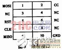
In addition, the module is also designed with a JTAG interface and an ISP programming interface (ISP is in-System Programmable). The JTAG interface can connect the microcontroller to the parallel interface of the microcomputer through the downloader. The ISP programming interface is used when downloading or reading the internal program of the chip. The meaning of each pin is shown in Figure 3. One of the feet is connected to the PB3 of ATmega8. 4, 6, 8, lO ground, 5 feet connected to PC6 of ATmega8, 7 feet connected with PB5 of ATMesa8, 9 feet connected with PB4 of ATmega8.
2.2 Downloader Module
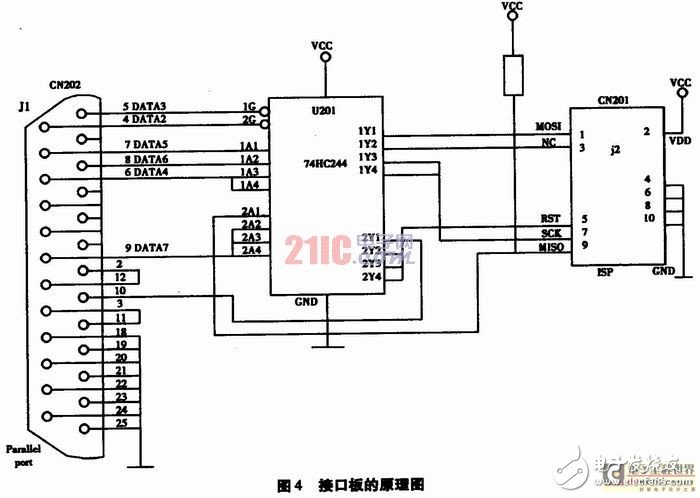
The downloader consists of an interface board and a connecting cable. The schematic diagram of the interface board is shown in Figure 4. In the figure, U201 is an 8-buffer 74HC244 circuit used as a buffer isolation for the parallel port of the computer and the microcontroller. The connector CN202 is a general-purpose DB25 pin plug, which is connected to the host computer for communication; 4 and 5 feet control the U201 chip, allowing normal data transmission when it is low level, and 74HC244 output is high impedance when high level; 7 feet Output data to the microcontroller; 6 feet are the clock signal; 9 feet are the output reset signal; 10 feet are the data read from the microcontroller. The download cable is a 10-core flat cable with an IDC plug on both ends. Connect the downloader to one end and the ISP port JP1 on the minimum system board. Collection
Comments (0)
share to
2.3 experiment instrument other circuit design
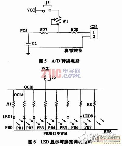
2. 3. 1 A/D conversion circuit
Figure 5 shows the A/D conversion circuit. The ATmega8 has a 1O-bit precision A/D converter with an accuracy of ±2LSB and a nonlinearity of O. 5 LSB, the conversion time is 65μs~260μs, the conversion precision of PC0~PC3 analog input channel is 10 bits, the conversion precision of PC4~PC5 analog input channel is 8 bit, the experiment instrument uses PC5 input, the reference voltage Vref is provided by chip inside. The reference voltage is grounded externally with capacitors C5 and C6 to increase the immunity of the ADC section. The input voltage can be changed by adjusting W1. CZ4 is an external A/D conversion interface.
Collection
Comments (0)
share to
LinkedIn2.3.2 LED display and pulse width modulation circuit
In order to meet the student's basic I / O port design requirements, the LED / LCD display interface circuit and pulse width modulation circuit are extended on the experimental instrument, as shown in Figure 6.
The pulse width modulation circuit utilizes an output terminal OC2 of the ATmega8 microcontroller, which is the second function of the PB3 pin and can be used as a compare match output or a PWM output. Disconnecting jumper J6 on the board is the output of the PWM. In addition to directly driving the PWM drive signal of the DC motor, the output PWM can also be used for digital/analog conversion by RC smoothing. In addition, with PWM driving, the power consumption of power semiconductor devices is much lower than that of analog signals.
2.3.3 Design of I2C Circuit and Serial Interface
The I2C circuit is formed by connecting the AT24C02 chip to the serial TWI bus (PC4, PC3). PC4 is the SCL clock line, PC2 is the SDA data line, and the I2C bus is formed by the AT24C02 chip 1/4 (not shown). The serial interface circuit is divided into the communication interface with the PC and the communication interface between the two MCUs. See CZ3 (CON3 MCU serial communication interface) and CZ4 (CON2 MCU and PC serial communication interface) in Figure 7. CZ2 is an RS232 interface, which can be used for asynchronous serial UART communication between PC and ATmega8. It can use PC screen as user display terminal, which can make full use of PC resources.
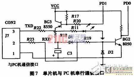
RS-232 interface cable is used when communicating with the computer using this interface. RS-232 is a single-ended signal transmission, suitable for short-distance or modem communication.
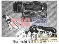
After the design of the above circuit, the PCB board is completed according to the circuit principle, and the experimental instrument hardware development board formed by welding the corresponding components and debugging is shown in FIG. 8 .
3 BASCOM-AVR integrated development software
ATMEL's AVR family of single-chip microcontrollers is based on the new reduced instruction RISC architecture, which was developed to enable high-level language programming to efficiently target products. At present, many companies in the world have launched AVR development software and platforms based on advanced programming languages ​​such as C and Basic. Based on ATmega8, the experimental development board uses BASIC
Language is a means of development platform - BASCOM-AVR. Its program design is simple and convenient, it is dedicated to various general-purpose interfaces, and has powerful functions, real-time graphical simulation platform, etc., and the advantages of AVR single-chip microcontroller program memory can be programmed online for multiple downloads. Making learning and using AVR single-chip microcontrollers is easy.
4 Summary and outlook
Based on the ATmega8 single-chip microcomputer experimental instrument integrated LCD liquid crystal display module, LED digital tube display module, keyboard module, A / D and D / A conversion module, general I / O interface module, communication interface module and other common experimental modules, using AVR microcontroller The basic system of experiments can be developed to complete some basic experiments to meet the requirements of students' basic experiments. At the same time, there is reserved space between the boards to meet the students' practice of innovative design, comprehensive curriculum design, extracurricular scientific activities and graduation design. The training activities require that the experimental system be tested by the electromechanical professional 07, 08, and electronic technology 07 and 08 students, the effect is more significant. Not only has the laboratory been moved into the dormitory, but also stimulated students' interest in learning, cultivated students' practical ability and innovative ability, and laid a solid foundation for quick adaptation to work in the future.
Fiber Optic Patch Panel,Fiber Patch Panel,Fiber Distribution Panel,Optical Patch Panel
Cixi Dani Plastic Products Co.,Ltd , https://www.dani-fiber-optic.com