Energy issues are a hot issue in the world today, and researchers in various countries have been working hard to find and develop new energy sources. In recent years, environmental vibration energy has become a “new darling†for researchers, and it has been applied to the power supply system of wireless sensor networks to replace traditional battery power.
Piezoelectric energy harvesting has become a hotspot in vibration energy collection research because of its many advantages such as high conversion efficiency, simple structure, and easy realization of miniaturization of the mechanism. However, piezoelectric ceramic sheets can only output low-power, low-current alternating current in a vibrating environment, and cannot directly supply power to electronic devices. It is often necessary to design additional energy harvesting circuits to perform AC and DC conversion and energy storage. How to improve the energy transfer efficiency of the energy harvesting circuit as much as possible is the main concern in this type of circuit research.
The earliest energy harvesting circuit consisted of diode bridge rectification and large capacitance filtering. It is known as the AC-DC standard energy harvesting circuit SEH (Standard Energy HarvesTIng), but the energy transfer efficiency of this circuit is low, especially for energy harvesting devices with low electromechanical coupling coefficient. To this end, Guyomar et al. proposed the Sxi (Synchronized Switch Harves TIng on Inductor), which has become a mainstream method for current energy harvesting circuit design because it can greatly improve energy transfer efficiency.
It should be pointed out that the principle of the traditional SSHI circuit is to close the switch to reverse the voltage when the vibration displacement reaches the maximum or minimum. In order to coordinate the control switch closure, it is necessary to use an externally powered sensor to detect the displacement and use the controller to control the switch. Obviously, this mode of operation consumes energy while collecting energy, which is contrary to the original intention of environmental energy harvesting. Aiming at this problem, this paper proposes a Self-Sensing Synchronized Switch Harvey TIng on Inductor (S-SSHI) that does not rely on external detection and control equipment. The advantage of this circuit is that it can be detected and controlled only by analog circuits, avoiding dependence on external devices and energy. In this circuit, the piezoelectric piece is both an energy harvesting component and a sensing component, and the closing timing of the switch can be automatically controlled by the peak detection and comparison of the output voltage. At the same time, an analog electronic switching technology is used to achieve switch closure. The working principle and power analysis of the circuit are given in the paper. Theoretical and experimental studies show that the SS-SSHI circuit can significantly improve the energy collection efficiency and avoid the dependence on external equipment and energy compared with the standard circuit.
1 Piezoelectric vibrator electrical model
The electrical model of the piezoelectric vibrator can be equivalent to a current source and an equivalent capacitor in parallel, as shown in Figure 1. In the figure, Cp is the clamping capacitance of the piezoelectric piece, Rp is the equivalent internal resistance of the piezoelectric piece, generally several tens of megaohms or more, and ieq is the equivalent current source current, which can be regarded as a constant current source.
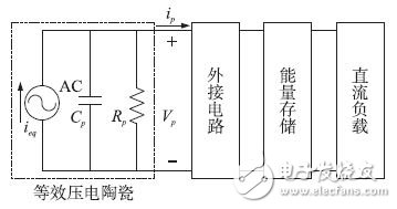
Figure 1 Piezoelectric energy harvesting model
Assuming that the current of the equivalent current source of the piezoelectric vibrator is ieq, then its relationship with the vibration speed is as follows:
Where αe is the external force-voltage factor and x(t) is the piezoelectric oscillator displacement.
2 piezoelectric vibrator electrical model
Piezoelectric vibrators generally produce alternating current, and most of the load we need to supply is DC, which requires rectification before powering the external load. Improving energy harvesting efficiency is the primary consideration in this type of circuit design. The problem.
2.1 Standard energy harvesting circuit
The standard energy harvesting circuit SEH (Standard Energy HarvesTIng) is the most common conversion circuit. It consists of a standard rectifier circuit and a filter capacitor. The filter capacitor C r is generally selected to be large enough to ensure that the rectified voltage V DC is a constant DC voltage, that is, the time constant RCr is much larger than the oscillation period. The circuit schematic is shown in Figure 2.
In the figure, C r is the filter capacitor, RL is the equivalent load, and the output power of the circuit is equal to the input power of the load. If the piezo voltage is | Vp| DC, then when | Vp | reaches VDC, the rectifier bridge turns on and the piezo voltage stops rising at | Vp | = VDC. When |Vp | begins to fall, the rectifier bridge begins to open again and the circuit is disconnected.
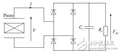
Figure 2 standard energy harvesting circuit
The relationship between voltage and power across the capacitor is:
q =C â— V (2)
Where q is the charge across the capacitor, C is the size of the capacitor, and V is the voltage across the capacitor.
When the voltage across the capacitor is a fixed value, the energy W stored on the capacitor is:
W =V â— q (3)
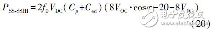
According to (2) and (3), it can be concluded that the energy harvesting power PSEH of the standard circuit is:
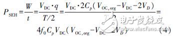
Here f0 = ω/2π is the vibration frequency, Cp is the piezoelectric element clamping capacitance, VDC is the rectified DC voltage, VOC, org is the original open circuit voltage amplitude, and VD is the diode voltage drop.
2.2 Inductor synchronous switch energy harvesting circuit
The traditional classic energy harvesting circuit has a large loss in the circuit itself due to the circuit being in the path state, and the structural defects of the circuit itself result in low energy collection efficiency. In order to solve this problem, the researchers proposed an energy-synchronized switch SSHI (Synchronized Switch Harvesting on Inductor) based on the inductor, the circuit includes an electronically controlled switch, when the displacement of the piezoelectric structure reaches the maximum or minimum value. The switch is triggered, and studies have shown that the energy harvesting efficiency of the SSHI circuit is much higher than that of the standard circuit. This type of circuit is further divided into a parallel synchronous switching circuit (P-SSHI) and a series synchronous switching circuit (S-SSHI).
The schematic diagram of the traditional SSHI circuit is shown in Figure 3. The circuit is disconnected most of the time, so the loss of the energy acquisition circuit itself is relatively small, which can improve the energy collection efficiency. The switch only closes when the displacement reaches the maximum or minimum value. At this time, an L-Cp oscillation circuit is formed. The circuit oscillation period is much smaller than the mechanical oscillation period. After each switch is closed, the energy stored on the piezoelectric piece Cp passes. The rectifier bridge and inductor L are transferred to the capacitor Cr.
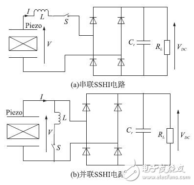
Figure 3 Schematic diagram of the traditional SSHI circuit
The equivalent current ieq and speed can be known by (1) ![]() Proportional, these switching actions ensure that Vp and ieq are in phase, so the input energy from the mechanical part to the electrical part is always positive. Lefeuvre et al. studied the maximum output power of SEH circuits and S-SSHI circuits:
Proportional, these switching actions ensure that Vp and ieq are in phase, so the input energy from the mechanical part to the electrical part is always positive. Lefeuvre et al. studied the maximum output power of SEH circuits and S-SSHI circuits:
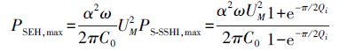
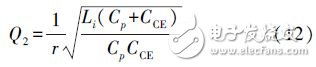
Where α is the force factor, ω is the vibration angular frequency, C0 is the piezoelectric element clamping capacitance, UM is the piezoelectric element vibration displacement amplitude, and Qi is the SSHI circuit quality factor.
It can be seen from the above equation that the maximum output power of the S-SSHI circuit is (1+e-Ï€/2Qi) / (1+e-Ï€/2Qi) times of the SEH circuit, which can obviously be significant by selecting the appropriate circuit quality factor Qi. Increase the maximum output power of the SSHI circuit.
3 self-sensing inductor synchronous switch energy harvesting circuit
However, the traditional SSHI circuit has a fatal disadvantage: it is not a self-sensing circuit, that is, the switching of the switch S, the need for displacement sensors and digital controllers, which require additional energy supply, contrary to the original intention of energy harvesting research. . Therefore, according to the electronic switch design given in [12] (Fig. 4), this paper proposes a Self-Sensing Synchronized Switch Harvesting on Inductor (SS-SSHI) method, which relies only on simulation. The circuit can automatically control the opening and closing of the switch according to the change of the output voltage of the piezoelectric element.
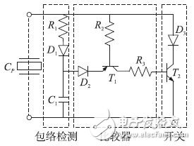
Figure 4 electronic switch
3.1 SS-SSHI circuit working principle
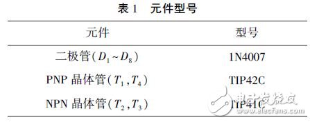
In the self-sensing synchronous switching circuit design, we use a complementary transistor topology to achieve direct envelope detection of the voltage Vp across the piezoelectric chip: one part is used for maximum detection and the remaining symmetrical part is used for minimum Detection. The improved circuit SS-SSHI for the SSHI circuit is shown in Figure 5. The main components of the figure are shown in Table 1.
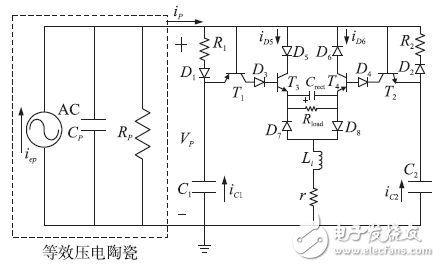
Figure 5 SS-SSHI circuit schematic
In the figure, Vp is the voltage across the piezoelectric ceramic chip, and VC1 and VC2 are the voltages across the capacitors C1 and C2, respectively. As with conventional SSHI circuits, the electronic switch closes when the voltage Vp reaches a maximum or minimum value with each change in vibration displacement during each cycle.
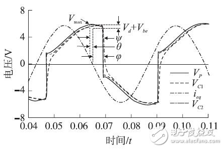
Figure 6 SS-SSHI circuit voltage curve
Since we are using a complementary topology, the maximum and minimum detections in the circuit are symmetrical. This article will focus on the principle of maximum detection (minimum detection is similar), combined with the four stages of circuit operation, gives the working characteristics of the SS-SSHI circuit. For maximum detection, switches R1, D1 and C1 form the envelope detector, T1 acts as the comparator and T3 acts as the electronic switch. The voltage changes in the four stages are shown in Figure 7.
Natural charging phase: When the circuit starts to work, since the voltage of the piezoelectric element increases from 0, there is a natural charging phase. The current trend during natural charging is shown in Fig. 8. The conduction portion of the circuit is the blue line in the figure. Only two envelope detector circuits are turned on at this stage, and all the transistors are turned off. The forward equivalent current ieq charges Cp, C1 and C2, so that Vp, VC1 and VC2 also grow simultaneously.
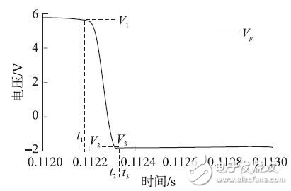
Figure 7 voltage Vp curve
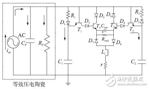
Figure 8 Natural charging
The first voltage inversion phase: When Vp reaches its maximum value Vmax, the voltage across capacitor C1 is Vmax -VD, where VD is the voltage drop across the diode. Then, Vp starts to fall. When the falling value reaches VD + VBE, that is, Vp = V1 (time T1), transistor T1 is turned on. Capacitor C1 begins to discharge through T1(ec), D3, T3(be), Crect, D8, Li, and r, and as a result, T3 is turned on. Inductive loops generated by switch T3: D5, T3(ce), Crect, D8, Li, and r cause a short circuit across Cp. Cp begins to discharge rapidly from voltage V1 through the inductive loop until Vp reaches its local minimum (time t2). The current flow of the first voltage inversion is shown in Figure 9, and the conduction portion of the circuit is the thick solid line in the figure.
Figure 9 First voltage flip
The second voltage inversion phase: the current through Li begins to flip its direction, but the T3 (ce) loop immediately blocks due to the current inversion of D5. However, the circuit consisting of D7, Cret, T4(ce) and D6 can still be turned on. Because even though T4 is open, there is always a small uncharged parasitic capacitance at its emitter and collector. The flip current passes through this loop until the emitter of the T4—collector capacitor CCE is fully charged. At this time (at time T3), Vp becomes V3. The local minimum of Vp, that is, V2, may cause a misjudgment of the minimum switch. Therefore, R2 is necessary to ensure that the discharge of C2 used for minimum detection is slower than Cp, so that the local minimum can be skipped. Figure 10 shows the current direction of the second voltage inversion, and the circuit conduction portion is indicated by a thick solid line. The second voltage inversion has side effects in the self-sensing energy harvesting circuit, and a small emitter-collector capacitor CCE can be chosen to avoid this effect. However, parasitic capacitance is always present in the actual triode.
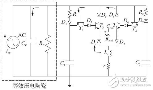
Figure 10 second voltage flip
Charge neutralization phase: After t3, both T3 and T4 are disconnected, but C2 still does not end discharge, and the remaining charge on C2 will flow into Cp and C1 until they have the same voltage. This charge neutralization causes Vp to increase by a point to V4 before entering the second half of the cycle, the minimum detection. The actual discharge of C2 starts from time t1, but for the sake of analysis, it is assumed that the charge neutralization phase is the same as the other three phases. The current trend of the charge neutralization phase is shown in Fig. 11, and the conduction part of the circuit is indicated by a thick solid line. .
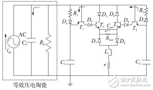
Figure 11 Charge Neutralization
The minimum switch detection can be done by the remaining symmetrical portion of the circuit, the principle of which is similar to the maximum value detection. For the minimum detection, the intermediate voltages become -V1, -V2, -V3 and -V4, respectively.
3.2 SS-SSHI Circuit Analysis
3.2.1 Switch phase delay
According to the principle analysis of the SSHI circuit in [7], the switching action should happen just when the voltage Vp reaches its extreme value, that is, Vmax or Vmin. However, in the SS-SSHI circuit, the switching action is just impossible at this moment. Due to the voltage drop of the diode and the triode in the envelope detector and the comparator, the switching action time and the maximum value (minimum value) Vp There is a phase delay between them. This phase delay can be seen as ψ in Figure 6, which can be calculated from:
![]()
From Fig. (6), it can be seen that the phase difference φ between the switching action time and the displacement maximum (ie ieq =0) is:

Where θ is the phase difference between the piezoelectric plate voltage maximum value Vp, oc and ieq's zero crossing point (from positive to negative). Obviously, this phase difference φ is variable, however it is considered constant in [15].
3.2.2 Voltage changes during circuit operation
In the traditional SSHI circuit, there are only two phases, the natural charging and voltage inversion phases, in one half of the vibration period. These two intermediate voltages can be calculated by charging and discharging in these two processes. In the SS-SSHI circuit, due to the interaction of the various stages in the self-sensing switching circuit, more stages need to be distinguished to better analyze the characteristics of the circuit. The four-stage circuit operation has been described above. From Figure 7, the voltages of the four phases vary from V1 to V4.
For the maximum value of the switch detection, if V1 》Vref1, then Vp begins to enter the first voltage flip. Here Vref1 is the reference voltage:
![]()
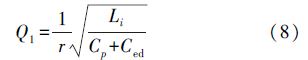
For the first voltage rollover (from V1 to V2), Cp, C1, Li and r form an RLC discharge loop with a quality factor of:
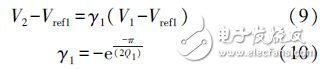
The relationship between V2 and V1 can be expressed as:
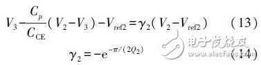
After the first rollover, if V2 "Vref2, Vp will flip again.
![]()
For the second flip (from V2 to V3), Cp, CCE, Li and r are connected in series to form an RLC discharge loop with a quality factor of:
You can get the relationship between V3 and V2:
Assuming that the discharge of C2 is after two flips of voltage Vp, charge neutralization can be considered as a separate phase. During the charge neutralization phase, the total charge on Cp, C1 and C2 is to be released. Considering the conservation of charge, the relationship between V4 and V1, V2, V3 is as follows:
![]()
After the charge neutralization is over, the natural charging phase begins again. During the remaining half of the cycle, the minimum switch begins to operate until Vp reaches -V1. Since the time of the two flip and charge neutralization phases is much less than half the vibration period, the value of Vp can be approximated as the value of Vp, oc at the switching instant, so the voltage relationship at this stage is as follows:
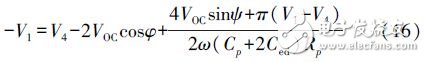
Combined with the linear equations (9), (13), (15) and (16), the solutions of V1 to V4 with respect to VOC and VDC can be derived.
3.2.3 Power Analysis
According to (2) and (3), the energy harvesting power of the SS-SSHI circuit can be found as:
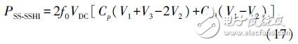
Here f0 = ω / 2π is the vibration frequency.
Since it is more difficult to accurately calculate the numerical solution of V1, V2, V3, and V4, the power is approximated by the equivalent method. Considering that the voltage changes in the third and fourth phases of the circuit are small, that is, V2 to V3 in Figure 7, the change of V3 to V4 is particularly small with respect to V1 to V2, so we can think of V2=V3 = V4. (17) can be approximated as:
![]()
Since the value of Rp is generally very large, tens of megabytes or more, (16) can be approximated as:
![]()
This can be combined with equations (9) and (19) to derive V1 and V2. Bring into equation (18) to derive the energy harvesting power of the SS-SSHI circuit.
4 Experiment and result analysis
4.1 Experimental system and experimental methods
In order to verify the energy harvesting effect of the SS-SSHI circuit, we designed the experimental system shown in Figure 12. The devices in the figure are 1. Function signal generator, 2. Oscilloscope, 3. Exciter, 4. Piezoelectric ceramic chip, 5. Exciter driving power supply, 6. Energy harvesting circuit.
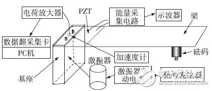
Figure 12 Energy Harvesting System
In the experiment, the harmonic excitation signal is first generated by the signal generator and input to the exciter driving power source for driving the exciter to vibrate at a certain frequency, which in turn drives the piezoelectric cantilever beam mounted on the exciter to vibrate. Through the positive piezoelectric effect, the mechanical energy is converted into electrical energy, and the energy harvesting circuit is used for energy harvesting. Finally, the energy harvesting effect is observed through an oscilloscope.
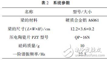
The main parameters of the whole system are shown in Table 2. Generally, in order to maximize the collected energy, it is selected to excite at the resonant frequency of the piezoelectric body (cantilever beam), at which time the piezoelectric body (cantilever beam) can generate more deformation and increase the output power. Since the natural mode of the cantilever beam is relatively high, in order to reduce the resonance frequency, a 10 gn mass (weight) is attached to the end of the cantilever beam in the experiment. In order to observe the energy harvesting efficiency under the resonance effect, the first-order modal frequency f = 22.3 Hz of the cantilever beam is selected as the frequency of the excitation source signal.
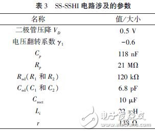
The specific parameters of the electronic components shown in Figure 5 are shown in Table 3. In the experiment, we simulate different loads by selecting resistors with different resistance values, and then observe the output of SS-SSHI circuit and SEH circuit at the load end through an oscilloscope. The voltages are such that their actual energy output power can be ascertained according to the theory described above.
table
4.2 Analysis of experimental results
We can observe the working state of the SS-SSHI circuit through the oscilloscope. The result is shown in Figure 13. The graph shows the variation curve of the voltage Vp across the energy collecting piezoelectric piece and the harmonic excitation signal input by the signal generator. The results show that the SS-SSHI circuit achieves voltage inversion at the maximum (minimum) displacement, meeting design expectations.
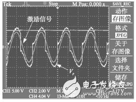
Figure 13 SS-SSHI circuit operating voltage curve
According to the foregoing theory, it is the main purpose of our research on energy harvesting circuits to increase the output power of the circuit as much as possible. Through equations (4) and (20) we can calculate the actual output power of the SEH circuit and the SS-SSHI circuit. However, it is necessary to know the phase difference φ when seeking the power of the SS-SSHI circuit. In order to measure this parameter, we affix two piezoelectric sheets symmetrically on the front and back sides of the cantilever beam, one of which is used for energy harvesting and the other is used as a sensor, and the output voltage is used to determine the moment corresponding to the displacement extreme value. The waveform of the two piezoelectric sheets can determine the value of φ. Through experiments, we find that the φ value changes slightly with the change of different loads, which is consistent with the assumption that φ is fixed in the literature [13]. The phase difference φ = 2π / 11 was measured in this experiment. Thus, according to equations (4) and (20), we can obtain the open circuit voltage amplitude VOC, and the theoretical power curve of the SS-SSHI circuit and the SEH circuit when org = 10.3 V is shown in Fig. 14.
In order to compare with the theoretical results, several resistors are used for experimental research. Different loads will cause the circuit to output different DC voltages VDC. According to the resistance value, the actual output power can be calculated by the formula P = U2 / R. Figure 14 shows that the measured power of the two circuits is in good agreement with the theoretical analysis results. In particular, the power theoretical calculation results of the SS-SSHI circuit are very close to the measured values.
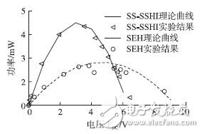
Figure 14 Theoretical and experimental power curves
In order to further compare the increase of output power of the acquisition circuit under different vibration levels, two sets of experiments were carried out with open circuit voltage VOC, org = 2.6 V and VOC, org = 6.5 V. The results are shown in Fig. 15.
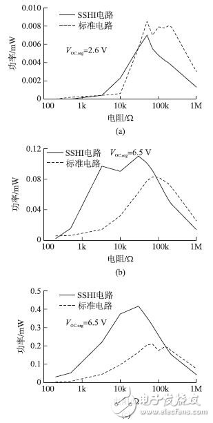
Figure 15 Energy harvesting power at different open circuit voltages
It can be seen from Fig. 15 that when the vibration amplitude is small, the open circuit voltage amplitude VOC at both ends of the piezoelectric piece is org = 2.6 V (Fig. 15(a)), and the SS-SSHI circuit reaches the maximum power at R = 50 kΩ. , ie 0.007 mW; while the SEH circuit R = 180 kΩ, the power reaches the maximum, ie 0.008 mW. It can be seen that the energy collection efficiency of the SS-SSHI circuit is similar to that of the SEH circuit. As the amplitude of the vibration increases, the open-circuit output voltage also increases, and the advantages of the SS-SSHI circuit gradually manifest. At VOC, org = 6.5 V, as shown in Figure 15(b), the SSSSHI circuit reaches its maximum power at R = 30 kΩ. : 0.110 4mW; while the SEH circuit R = 70 kΩ, the power reaches the maximum: 0.083mW. At this time, SS-SSHI is 33% higher than SEH energy harvesting power, while at VOC, org = 10.3 V, as shown in Figure 15(c), the SS-SSHI circuit reaches its maximum power at R = 30 kΩ: 0.415 4 mW; The maximum power is reached when the circuit R = 70 kΩ: 0.208 5 mW. At this time, SS-SSHI is 99.23% higher than SEH energy harvesting power. It can be seen that the SS-SSHI circuit is more suitable for energy harvesting under high input voltage conditions.
5 Conclusion
Micro-energy has received more and more attention from people, and vibration energy has received much attention as the most common form of energy existence. Piezoelectric components are widely used in vibration energy harvesting due to their unique advantages.
In this paper, the electrical model equivalent modeling of the piezoelectric vibration energy harvesting system is firstly carried out, followed by a simple analysis of the working principle and acquisition efficiency of the traditional standard energy harvesting circuit SEH. The working principle of the SSHI circuit is briefly described and a self-sensing energy acquisition circuit SSSSHI is designed and implemented for the disadvantage that its switching control requires additional functions. This SS-SSHI circuit can realize the self-switching of the switch without any external energy supply. When the vibration displacement (voltage) reaches the maximum or minimum value, the switch opens so that the energy on the piezoelectric element flows through the rectifier bridge. Load to achieve the purpose of energy harvesting. Through theoretical analysis and experimental verification, this SS-SSHI circuit can significantly improve the energy harvesting power. At VOC, org = 10.3 V, SS-SSHI increases the power of SEH energy by 99.23%. The experiment also shows that the energy harvesting power of the SS-SSHI circuit can be significantly improved compared to the energy harvesting power of the SEH circuit at large input voltages.
Trolley Dj Speaker,Bluetooth Speaker Price,Bluetooth Trolley Speaker,Outdoor Bluetooth Speakers
Newmax Electronics Co.,LTD , https://www.fspeaker.com