Abstract: The 8-bit CMOS microcontroller rfPIC12C509AF has TISC central processor, 1024 & TImes; 12bit programmable EPROM, 41 bytes of data RAM, 8-bit programmable timer / counter, watchdog timer, 5 general-purpose I / O circuits The radio frequency range of embedded UHF ASK / FSK transmitter is 310 ~ 480MHz, output power + 2 ~ -12dBm, ASK data transmission rate is 0 ~ 40Kbps, FSK data transmission rate is 0 ~ 20Kbps, PLL is phase locked. This article briefly introduces the features and application circuits of rfPIC12C509AF.
1 Overview
tfPIC12C509AF is an 8-bit CMOS microcontroller with a single-chip integrated RF wireless data transmitter embedded by Microchip. The chip has a high-performance RISC central processor, 33 12-bit word-length instructions, 8-bit word-length data; built-in 4MHz RC oscillator, operating speed 1μs instruction cycle; 7 special function hardware registers, 2 level hardware stack , Direct, indirect and relative addressing; 1024 & TImes; 12bit programmable EPROM, 41 bytes of data RAM; online serial programming (In-Circuit Serial ProgrammingTM, ICSP TM), frequency programmable calibration of the internal RC oscillator (independent Transmitter quartz crystal oscillator reference), 8-bit programmable timer / counter; power-on reset, watchdog timer, low-power sleep mode, programmable code protection, 5 general-purpose I / O and other functions; work The voltage is 2.5 ~ 5.5V, and the low current consumption sleep mode current is 0.2 ~ 4μA. Embedded UHF ASK / FSK transmitter, RF frequency range is 310 ~ 480MHz, adjustable output power + 2 ~ 12dbm, ASK data transmission rate 0 ~ 40Kbps, FSK data transmission rate 0 ~ 20Kbps, PLL phase lock, integrated Crystal oscillators and VCO circuits require only a few external components.
It can be used in remote keyless entry (RKE) transmitters, garage door openers, telemetry (tire pressure, water, electricity, gas meters, valuables tracking), wireless security systems, radio remote control and other fields. 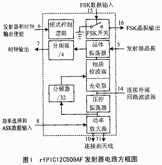
2 Pin arrangement and function
rfPIC2C509AF is packaged in a 20-pin SSOP. The functions of each pin are as follows.
1 (VDD): logic circuit and I / O terminal products / quartz oscillator input / external clock input (GPIO is only in internal RC mode, OSC1 in other oscillator modes). TTL input when GPIO, ST input when in external RC oscillator mode.
3 (GP4 / OSC2): bidirectional I / O terminal product, quartz crystal oscillator output. Connect the crystal or resonator in the quartz crystal oscillator mode.
4 (GP3 / MCLR / VPP): input port / user clear (reset) input / program voltage input. When MCLR is formed, this pin is active low to realize device reset. When the device enters normal operation and programming mode, the voltage on MCLR and VPP cannot exceed VDD, and can change the pin state through software programming to wake up the sleep state.
5 (XTAL): Transmitter crystal oscillator connected to COPITTS crystal oscillator.
6 (RFENIN): transmitter and clock output enable, internal pull-down.
7 (CLKOUT): clock output.
8 (PS / DATAASK): power selection and ASK data input. 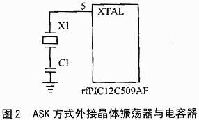
9 (VDDRF): Positive voltage terminal of the transmitter.
10 (ANT1): The output of the differential power amplifier is connected to the antenna, and the open collector output.
11 (ANT2): The output of the differential power amplifier is connected to the antenna, and the open collector output.
12 (VSSRF): ground reference terminal of the transmitter.
13 (NC): empty foot.
14 (LF): Connect the external loop filter. The common point of VCO conversion input and charge pump output.
15 (DATAFSK): FSK data input.
16 (FSKOUT): The output of FSK crystal oscillator.
17 (GP2 / T0CKI): Bidirectional I / O port, which can constitute T0CKI.
18 (GP1): bidirectional I / O port / serial port programming clock, which can wake up the sleep state by changing the pin state through software programming. This buffer is a Schmitt trigger input in serial programming mode.
19 (GP0): bidirectional I / O port / serial port programming data, which can wake up the sleep state by changing the pin state through software programming. This buffer is a Schmitt trigger input in serial programming mode.
20 (VSS): Reference ground for logic circuits and I / O pins.
3 Basic structure and characteristics
The internal structure of rfPIC12C509AF includes a complete 8-bit CMOS microcontroller circuit and transmitter circuit. The transmitter circuit is described below. The block diagram of the transmitter circuit is shown in Figure 1. 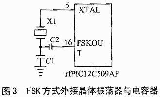
The transmitter is a complete integrated UHF ASK / FSK transmission circuit, which consists of a quartz crystal oscillator, a phase-locked loop circuit (PLL), an open collector output power variable amplifier PA (Power Amplifier) ​​and mode control logic ). The external components include bypass capacitor, crystal oscillator and PLL loop filter, which can realize the operation of ASK and FSK.
Pins VDDRF and VSSRF are the power supply terminal and ground terminal of the transmitter circuit, respectively. These power pins are independent of the power supply pins VDD and VSS of the microcontroller.
The transmitter's quartz crystal oscillator is a Kobeci oscillator, which provides the reference frequency of the PLL and is independent of the oscillator of the PIC microcontroller. Connect external oscillator or AC analog reference signal to XTAL pin. The transmission frequency is determined by the crystal frequency, the formula is as follows:
ftransmit = fXTAL & TImes; 32
Considering the flexible selection of the transmission frequency, the final crystal frequency may not be the standard value. The minimum value of the crystal frequency is 9.65 ~ 15MHz, the load capacitance is 10 ~ 15pF, the parallel capacitance is 7pF, and the equivalent series impedance is 60Ω.
rfPIC12C509AF crystal oscillator realizes ASK operation circuit as shown in Figure 2. Capacitor C1 takes a value of 22 ~ 1000pF.
rfPIC12C509AF crystal oscillator realizes FSK operation circuit as shown in Figure 3. Capacitors C1 and C2 achieve FSK modulation by dragging the crystal oscillator. When DATAFSK = 1, FSKOUT is high impedance, only C1 is used for the crystal oscillator, and the transmission frequency is fMAX; when DATAFSK = 0, FSKOUT and VSSRF are grounded, capacitors C1 and C2 are connected in parallel, and the transmission frequency is fMIN. Choose an ideal set of C1 and C2 values ​​to determine the center frequency and frequency deviation. Capacitor C1 determines fMAX and the parallel value of capacitors C1 and C2 determines fMIN.
The value of C1 is 22 ~ 1000pF, and the value of C2 is 47 ~ 1000pF.
Transmitter center frequency (fc): fc = (fMAX + fMIN) / 2
Transmitter frequency deviation: Δf = (fMAX-fMIN) / 2
The quartz crystal oscillator has a Divide by 4 circuit. This circuit outputs the clock through the clock output (CLKOUT) pin. The CLKOUT clock output signal can be used as an input to a microcontroller or a stable reference frequency for other peripheral circuits. Be careful not to connect the CLKOUT signal to the PIC microcontroller's OSC1 input, because the PIC microcontroller cannot work without a clock signal, and the transmitter's oscillator cannot work at this time. At this time, the PIC microcontroller needs to introduce a clock from the outside or generate a clock through the internal RC oscillator. When a stable reference frequency is required in the application, the CLKOUT pin can be connected to the GP2 / T0CKI input and the TIMER0 module can be used. In order to make the interference signal habits as small as possible, there should be a rate limit for CLKOUT. The voltage amplitude of CLKOUT is determined by the charging capacitor on the CLKOUT pin (2VPP, 5pF).
A phase-locked loop circuit (PLL) is composed of a phase frequency detector, a charge pump, a voltage controlled oscillator VCO (Voltage Controlled Oscillator), and a fixed divide by 32. Pin LF is connected to an external loop filter. This loop filter controls the dynamic range and initial lock time of the PLL.
The output of the PLL gives power to the amplifier (PA). Different values ​​of the open collector output can directly drive the closed-loop antenna (ANT1, ANT2) or change to a single-port output through an impedance matching network or balun. Pins ANT1 and ANT2 are open collector outputs and must be pulled up to VDDRF through the load.
The differential output of the PA should match a 1kΩ load resistor. When the matching is not reasonable, it will cause excessive interference and harmonic radiation. The transmit output power can be adjusted to 6 equal values ​​in + 2 ~ -12dBm by changing the voltage of the PS / DATAASK pin.
In FSK operation, the PS / DATAASK pin can only be used as a power selection pin (PS). An internal current source output current of 20μA flows into the PS / DATAASK pin, and a voltage drop is generated through the resistor R2, which is used as a power control voltage (VPS) to control the transmit output power. VPS controls the bias current of the PA, and high transmit power requires a large bias current.
In order to realize ASK operation, the function of the PA / DATAASK pin is to control the power amplifier PA to be turned on or off. R1 and R2 on the voltage divider network are to determine the VPS in order to achieve the purpose of selecting the output power of the transmitter. If you want to get the maximum transmitter output power, you can directly connect the pin GP0 and PA / DATAASK.
The logic control mode pin RFENIN controls the operation of the transmitter. When RFENIN = 1, the transmitter and CLKOUT are in the working mode; when RFENIN = 0, the transmitter and CLKOUT enter the standby mode. In standby mode, the transmitter generates very little current. The REFNIN pin has an internal pull-down resistor. 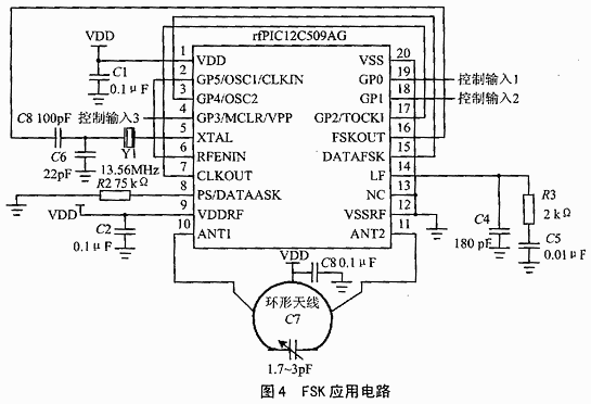
4 Application circuit
An FSK application circuit is shown in Figure 4, with an operating frequency of 433.92MHz and an output power of + 2dBm. The circuit can transmit the data in the microcontroller according to the control input signal.
When designing a printed circuit board, it should be noted that it is necessary to provide a low impedance power supply and a ground wire for minimum noise radiation. It is required to use a double-sided PCB and place the ground plane on the bottom layer to reduce radio radiation and crosstalk; the bypass capacitor should be as close as possible to each power supply pin VDD and VDDRF; use a separate PCB via to connect VSS and VSSRF Do not connect the PCB through-hole to the complex ground wire; in order to reduce the distributed capacitance in the circuit, the occurrence of parallel lines should be avoided; the shorter the line, the better; to prevent coupling, the components should be independent; use grounding The line isolates each signal; shields the clock output line with a ground wire to isolate the CLKOUT signal and reduce coupling; the component of the loop filter is placed as close as possible to the LF pin, and the line is kept as short as possible; the transmitting antenna can be printed On the PCB.
Acid Filling Machine,Battery Acid Filling Machine,Acid Filling Machine Battery,Quality Acid Filling Machine
Zhijiang BSL battery technology service company , https://www.bslbatteryservice.com