The synchronization module is the heart of each system, and it feeds the correct clock signal to every other module in the system. Therefore, special attention needs to be paid to the design and implementation of the synchronization module. This article examines the clock characteristics that affect system design and evaluates the causes of signal degradation. This article also analyzes the impact of the deterioration of synchronization and discusses the requirements of standards developed by the standardization organization to ensure transmission quality and interoperability of various transmission equipment.
Summary:
Network synchronization and clock generation are important aspects of high-speed transmission system design. In order to improve network efficiency by reducing transmission and reception errors, the quality of the clocks used at all stages of the system must be maintained at a specific level. The network standard defines the architecture of the synchronous network and its expected performance on the standard interface to ensure transmission quality and seamless integration of transmission equipment. There are a large number of synchronization issues, and system designers must be very clear when establishing system architecture. This article discusses various sources of clock degradation, such as jitter and drift. This article also discusses the causes and effects of clock degradation in the transmission system, analyzes the standard requirements, and proposes various implementation techniques.
Basic concept: jitter and drift <br> The general definition of jitter can be "a brief deviation of an event from its ideal appearance". In digital transmission systems, jitter is defined as a momentary change in the important moment of a digital signal from its ideal position in time. The important moment may be the best sampling moment of a bit stream with a period of T1. Although it is expected that each bit will appear at an integer multiple of T, it will actually be different. This pulse position modulation is considered to be a kind of jitter. This is also called the phase noise of the digital signal. In the figure below, the actual signal edge moves periodically around the ideal signal edge, demonstrating the concept of periodic jitter.
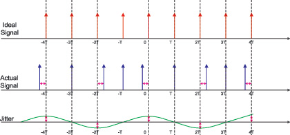
Figure 1. Illustration of jitter
Jitter, unlike phase noise, is expressed in units of intervals (UI). One unit interval is equivalent to one signal period (T), which is equal to 360 degrees. Assuming that the event is E, the nth occurrence is represented as tE [n]. Then the instantaneous jitter can be expressed as:
A set of peak-to-peak jitter values ​​including N jitter measurements is calculated using the minimum and maximum instantaneous jitter measurements as follows:

Drift is low frequency jitter. The typical dividing point between the two is 10 Hz. The effects of jitter and drift will appear in different but specific areas of the transmission system.
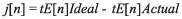
Types of jitter <br> According to the causes, jitter can be divided into two main types: random jitter and deterministic jitter. Random jitter, as its name implies, is unpredictable and is caused by random noise effects such as thermal noise. Random jitter usually occurs during the edge transition of a digital signal, causing random intersecting intervals. There is no doubt that random jitter has a Gaussian probability density function (PDF), which is determined by its mean (μ) and root mean square (rms) (σ). Since the tail of the Gaussian function extends infinitely on both sides of the mean, instantaneous jitter and peak-to-peak jitter can be infinite. Therefore, random jitter is usually expressed and measured using its root mean square value.
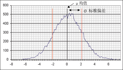
Figure 2. Random jitter expressed as a Gaussian probability density function
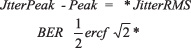
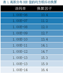
For jitter margin, peak-to-peak jitter is more useful than root-mean-square jitter, so the rms value of random jitter needs to be converted to peak-to-peak. To convert the root-mean-square jitter to peak-to-peak jitter, an arbitrary limit of the random jitter Gaussian function (arbitrary limit) is defined. Bit error rate (BER) is a useful parameter in this conversion. It assumes that bit errors occur when the instantaneous jitter in the Gaussian function falls outside its mandatory limit. Through the following two formulas, you can get the conversion of rms jitter to peak-to-peak jitter. 3
The following table can be obtained from the formula. The peak-to-peak jitter in the table corresponds to different BER values.
Deterministic jitter is bounded, so it can be predicted and has a certain amplitude limit. Considering integrated circuit (IC) systems, there are a large number of process, device, and system-level factors that will affect deterministic jitter. Duty cycle distortion (DCD) and pulse width distortion (PWD) will cause distortion of the digital signal, causing the zero-crossing interval to deviate from the ideal position and move up or down. These distortions are usually caused by the timing difference between the rising and falling edges of the signal. If there is a ground potential drift in the unbalanced system, there is a voltage offset between the differential inputs, and the rise and fall time of the signal changes, etc., it may also cause this distortion.
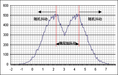
Figure 3. Dual-mode representation of total jitter
Data-dependent jitter (DDJ) and inter-symbol interference (ISI) cause signals to have different levels of zero-crossing intervals, resulting in different signal transitions for each unique bit pattern. This is also known as mode dependent jitter (PDJ). The low-frequency cutoff point and high-frequency bandwidth of the signal path will affect the DDJ. When the bandwidth of the signal path can be compared with the bandwidth of the signal, the bit will extend into the adjacent bit time, causing inter-symbol interference (ISI). The low-frequency cutoff point will distort the signal of the low-frequency device, and the system's high-frequency bandwidth limitation will degrade the performance of the high-frequency device. 7
Sinusoidal jitter modulates the signal edges in a sinusoidal pattern. This may be due to power supply to the entire system or even other oscillations in the system. Ground bounce and other power supply changes may also cause sinusoidal jitter. Sinusoidal jitter is widely used in the testing and simulation of jitter environments. Unrelated jitter may be caused by power supply noise or crosstalk and other electromagnetic interference.
When considering the impact of jitter on digital signals, the entire deterministic jitter and random jitter need to be considered. The sum of deterministic jitter and random jitter will produce another probability distribution 4: dual-mode response, where the middle represents deterministic jitter and the tail is Gaussian response, representing random jitter components.
Jitter measurements — TIE, MITE and TEDV
Time interval error (TIE) is obtained by measuring the actual clock interval and the same interval of the ideal reference clock. At a given time t, a clock of time T (t) is generated at a time interval called the observation interval, and its TIE relative to the clock Tref (t) can be expressed by the following formula. (X (t) is called the error function.)
TIE represents the high-frequency phase noise in the signal and provides direct information that the actual clock deviates from the ideal situation every cycle. TIE is used to calculate a large number of statistical derived functions such as MTIE, TDEV, etc.
The maximum time interval error (MTIE) is defined as the maximum peak-to-peak delay change of a given clock signal relative to an ideal clock signal within an observation time (t = nt0), where all observation times of this length are being measured Within the period (T). Use the following formula to estimate:
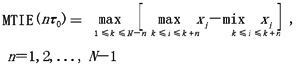
MTIE is defined for the slow change or drift of time. When you need to analyze the long-term characteristics of the clock, you need to measure MTIE. The MTIE value is a measure of the long-term stability of a clock signal.
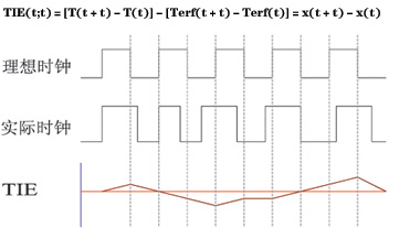
Figure 4. Graphical representation of TIE
TDEV is another statistical parameter that measures the expected time change of a signal as a function of integration time. DEV can also provide information about the phase (time) noise spectral components of the signal. The standard deviation of each point in the TIE graph is calculated for an observation interval that slips across the entire measurement time. This value is averaged throughout the above measurement time to obtain the TDEV value for this specific interval. Increase the observation interval and repeat the measurement process. TDEV is a measure of short-term stability and is useful when evaluating clock oscillator performance. TDEV is a unit of time.
Causes of jitter and drift in high-speed transmission systems <br> The most commonly used clock architecture is to run a low-frequency clock on the standby board to generate a synchronized high-frequency clock on each transmission card. The low-frequency clock is multiplied in the integrated circuit or through a discrete PLL to generate a high-frequency clock. With typical PLL frequency multiplication, the phase noise on the clock after frequency multiplication increases to the power of 20 * log (N) of the original clock phase noise, where N is the frequency multiplication factor. In addition, the jitter on the PLL reference clock input will extend the lock time, and the high-speed PLL cannot even achieve lock when the input jitter is too large. Using a higher-speed differential clock on the standby board will have better jitter performance than using a low-speed single-ended clock.
Because the VCO is more sensitive to input voltage changes, power supply noise is a major factor in increasing clock jitter. The output clock jitter amplitude is proportional to the power supply noise amplitude and VCO gain, and inversely proportional to the noise frequency. The drop in resistance due to the wire resistance and the power or ground bounce caused by the inductive noise formed by the wire inductance will have a similar effect on the above output clock jitter. Fully filter the power supply on the system board, and provide decoupling capacitors near the power supply pins of the integrated circuit to ensure higher jitter performance of the PLL.
In the system board, the clock and data are independent of each other, and changes in the start-up, hold-up, and delay times at the transmitting and receiving ends are critical to high rates. Differences in propagation delay between data and clock paths due to the presence of different active components in the data and clock paths, wiring delay differences between clock paths, wiring delay differences between data bits, and differences between data and clock paths Load conditions, packet length differences, etc., may all cause the above changes. When planning system jitter margins, changes in different signal paths must be taken into account.
When transmitting over a distance, there is accumulation of jitter at many points in the transmitter and receiver. In the transmitter physical layer implementation, nonlinear characteristics such as DAC nonlinearity or laser nonlinearity will aggravate signal distortion. In transmission media and receivers, in addition to external spurious sources (mostly in copper wires), fiber distortion due to different frequencies and modulation effects, due to receiver implementation (mainly related to bandwidth) and clock extraction circuit implementation The resulting signal-related phase deviation will increase the jitter of the signal flow.
Figure 5. MTIE deviation from TIE graph
Specific to SDH (Synchronous Digital Series) transmission, a large number of system-level events can cause jitter. In a typical transmission system that maps PDH (quasi-synchronous digital series) branches to SDH frames and transmits them through SDH NE (network components), before the PDH branch is demapped by the SDH terminal multiplexer, VC (Virtual Container) resynchronization occurs at an intermediate node. The gapped clock is used to map each branch to and from the STM-N frame, and emit pulses corresponding to the overhead, fixed padding, and adjustment bits, thus causing mapping jitter. The method of adjusting the chance bit to compensate the frequency deviation in the PDF branch will cause latency jitter. There is also a pointer adjustment mechanism to compensate for phase fluctuations between the input VC from the initial NE and the locally generated output STM-N frame. According to the frequency deviation, the VC moves back and forth in the STM-N frame. This will cause the VC extraction point to see sudden changes in the bitstream, resulting in a type of jitter called pointer jitter. All of the above system-level jitter will increase the total deterministic jitter.
Although all the above factors will increase the jitter of the signal propagation from the source to the destination, the standard requirements still specify that the transmission point needs to have a lower jitter value than the theoretical value. In this way, the clock driving the signal at the source will have a relatively low jitter value, taking into account the effects of clock multiplication, power supply changes, electrical-optical-electrical conversion, transmission and reception effects, and other distorted signals that deteriorate the actual signal. .
The effect of jitter on the transceiver <br> Ideally, the digital signal is sampled at the midpoint between two adjacent level shift points. The reason why jitter causes bit errors is that it changes the edge transition point of the signal relative to the ideal midpoint. The bit error may be caused by the edge of the signal flow changing too late (0.5 UI later than the ideal midpoint in time (unit interval corresponds to one cycle of the signal)) or too early (0.5 UI earlier than the ideal midpoint in time). When the clock sampling edge misses 0.5UI on either side of the signal flow, a 50% error probability will occur, assuming an average conversion density of 0.5. 7 If you know deterministic jitter and random jitter separately, you can pass the A table that associates the peak-to-peak jitter value with the root mean square jitter value to estimate the bit error rate. Calibration jitter, defined as the short-term change between the optimal sampling time of a digital signal and the sampling clock extracted from it, can cause the above-mentioned bit errors. For commercial applications, the source clock and source transmit interface jitter specifications will be much lower than 1UI.
The transmit interface jitter specification usually matches the input jitter tolerance at the receiving end. This is especially true for the jitter measurement loop filter cutoff frequency. For example, in an SDH system, there are two types of jitter measurement bandwidth, which are specified: one for wideband measurement filters (f1 to f4) and one for high-band measurement filters (f3 to f4). The value f1 refers to the narrowest clock cutoff frequency of the output clock signal that can be used in the PLL of the line system. Jitter at frequencies below this bandwidth will pass through the system, while jitter at higher frequencies will be partially absorbed. The value f3 represents the bandwidth of the input clock capture circuit. Jitter above this frequency will cause calibration jitter. Calibration jitter causes loss of optical power and requires additional optical power to prevent various deteriorations. Therefore, it is very important to limit the jitter of the high-band spectrum at the transmitter.
The effect of drift on the transceiver <br> Most telecom receivers on the market use a buffer to accommodate random fluctuations in the line signal. Block 6 below shows this concept in detail. The recovered clock sends data into a flexible buffer, while the system clock sends data out to the core of the device.
In a quasi-synchronous transmission system, the transmitter and receiver work at independent and extremely close frequencies, and fL and Fs represent the frequencies of the transmitter and receiver, respectively. When there is a phase or frequency difference between the two, elastic storage will eliminate it, otherwise the buffer will be underloaded or overflow (depending on the magnitude of the difference and the size of the elastic buffer), causing a controllable frame slip ( Basic rate transmission) or one bit adjustment (high-order asynchronous multiplexer).
In quasi-synchronous applications, frequency variation and buffer depth are standardized based on acceptable buffer slip. The original network was mainly used for voice transmission, and it would not cause voice quality degradation under a certain frequency threshold. The ITU-T specification specifies that the change is +/- 50ppm. But as the network began to transmit compressed voice, fax-formatted data, video, and other types of media applications, slippage severely reduced efficiency for errors and retransmissions, and the newly emerging synchronous network.
In a synchronous transmission system, the system clock is usually synchronized to the recovered clock of the interface used to receive signals of higher clock levels. The instantaneous and cumulative differences in phase and frequency between the recovered clock and the system clock will be absorbed by the elastic buffer, otherwise it will cause elastic memory overflow / underload (depending on the buffer size and the magnitude of the change), causing the pointer adjustment to be delayed or advanced Frame adjustment, frame slip, or bit adjustments occur somewhere in the system.
In a synchronous system, all network components work at the same average frequency, and frame deterioration can be eliminated through the pointer mechanism. These pointer mechanisms will advance or delay the position of the payload in the transmission frame, thereby adjusting the frequency and phase changes present in the receiving and system clocks. The buffer in the SDH transceiver is smaller than that in the PDH transceiver, and there are restrictions on irregularities such as pointer movement that may be caused in the SDH system. Therefore, compared with the PDH system, the synchronization system has stricter requirements. Due to the history of network development and interoperable connections between different networks, at certain stages or at other stages, these synchronized networks will be connected via quasi-synchronous networks. Therefore, the clock architecture of the PDH network should also be considered.
MTIE provides the peak time variation of the clock relative to a known ideal reference clock. The MTIE value will be used in the design of elastic buffers for synchronous transmission and switching equipment. In flexible storage, the buffer fill level is proportional to the TIE between the input digital signal and the local system clock. Ensuring that the clock complies with the MTIE clock specifications will ensure that certain buffer thresholds are not exceeded. Therefore, in the buffer design, its size depends on the specified limit of MTIE.
Figure 6. Receiver interface of a typical transmission system
The impact of system clock output phase disturbance on the transceiver <br> The output phase change of a clock can be obtained by analyzing its MTIE information. Drift generation (in free oscillation mode and synchronous mode) mainly refers to the long-term stability of the clock oscillator used in the system. In free oscillation mode, the stability of the system is only affected by the stability of the oscillator. In addition to drift generation, the output clock phase is also affected by a large number of system irregularities.
Especially for a system synchronizer, switching the reference source from a bad or degraded reference clock to a normal reference clock may cause output phase disturbances. The conventional VCO (voltage controlled oscillator) used in the high-speed PLL for transmission uses the method of switching the capacitor bank when changing the reference clock. This switching transition will cause a temporary phase shift of the output clock. Using ultra-low jitter clock multiplier circuit can solve this problem.
The high-performance network clock adopts a mechanism called "hold" when all the reference clocks of the system are lost. This is achieved by using the memory storage technology to generate the last known good reference clock of the system. Entering and exiting hold mode may cause phase disturbance to the output. When in hold mode, due to the inaccurate frequency regeneration, it will continue to produce output phase errors. Advances in integrated circuit technology have enabled maintaining accuracy to 0.01 ppb. Input reference clock deterioration and too little maintenance testing of the system (which will not cause reference clock switching) will also cause output phase disturbances.
The system output disturbance is limited and depends on the input tolerance that the system can accept at a lower level. For example, a clock that complies with G.813 option 1, the phase slope and maximum phase error allowed in the phase disturbance are limited to 1 μS, the maximum phase slope is 7.5 ppm, two 120 ns phase error segments, and the remaining phase slope is 0.05 ppm. These numbers correspond to the input jitter tolerance specified in the G.825 standard, which describes the control of jitter and drift within the SDH network.
When the output phase is disturbed, keeping the amplitude and rate of the phase error within the limits recommended by the standards organization can ensure that the signal degradation is properly handled in the end-to-end system to avoid data corruption or loss. For example, when the system synchronizer performs reference clock switching, if the output phase error is within specifications, the synchronizer can achieve "uninterrupted" reference clock switching, indicating the presence of buffer overflow or underload, causing pointer movement and bit adjustment Or swipe.
Conclusion <br> Network synchronization and clock generation are the most important parts of all high-speed transmission network systems. This article discusses the different types of clock degradation, mainly jitter and drift. The article also discusses in detail the causes of the above deterioration and how they affect the transmission system. Systematic design and implementation of the clock subsystem will improve the performance of the entire system, reduce the bit error rate, facilitate integration, and provide higher transmission quality and efficiency.
Summary:
Network synchronization and clock generation are important aspects of high-speed transmission system design. In order to improve network efficiency by reducing transmission and reception errors, the quality of the clocks used at all stages of the system must be maintained at a specific level. The network standard defines the architecture of the synchronous network and its expected performance on the standard interface to ensure transmission quality and seamless integration of transmission equipment. There are a large number of synchronization issues, and system designers must be very clear when establishing system architecture. This article discusses various sources of clock degradation, such as jitter and drift. This article also discusses the causes and effects of clock degradation in the transmission system, analyzes the standard requirements, and proposes various implementation techniques.
Basic concept: jitter and drift <br> The general definition of jitter can be "a brief deviation of an event from its ideal appearance". In digital transmission systems, jitter is defined as a momentary change in the important moment of a digital signal from its ideal position in time. The important moment may be the best sampling moment of a bit stream with a period of T1. Although it is expected that each bit will appear at an integer multiple of T, it will actually be different. This pulse position modulation is considered to be a kind of jitter. This is also called the phase noise of the digital signal. In the figure below, the actual signal edge moves periodically around the ideal signal edge, demonstrating the concept of periodic jitter.
Figure 1. Illustration of jitter
Jitter, unlike phase noise, is expressed in units of intervals (UI). One unit interval is equivalent to one signal period (T), which is equal to 360 degrees. Assuming that the event is E, the nth occurrence is represented as tE [n]. Then the instantaneous jitter can be expressed as:
A set of peak-to-peak jitter values ​​including N jitter measurements is calculated using the minimum and maximum instantaneous jitter measurements as follows:
Drift is low frequency jitter. The typical dividing point between the two is 10 Hz. The effects of jitter and drift will appear in different but specific areas of the transmission system.
Types of jitter <br> According to the causes, jitter can be divided into two main types: random jitter and deterministic jitter. Random jitter, as its name implies, is unpredictable and is caused by random noise effects such as thermal noise. Random jitter usually occurs during the edge transition of a digital signal, causing random intersecting intervals. There is no doubt that random jitter has a Gaussian probability density function (PDF), which is determined by its mean (μ) and root mean square (rms) (σ). Since the tail of the Gaussian function extends infinitely on both sides of the mean, instantaneous jitter and peak-to-peak jitter can be infinite. Therefore, random jitter is usually expressed and measured using its root mean square value.
Figure 2. Random jitter expressed as a Gaussian probability density function
For jitter margin, peak-to-peak jitter is more useful than root-mean-square jitter, so the rms value of random jitter needs to be converted to peak-to-peak. To convert the root-mean-square jitter to peak-to-peak jitter, an arbitrary limit of the random jitter Gaussian function (arbitrary limit) is defined. Bit error rate (BER) is a useful parameter in this conversion. It assumes that bit errors occur when the instantaneous jitter in the Gaussian function falls outside its mandatory limit. Through the following two formulas, you can get the conversion of rms jitter to peak-to-peak jitter. 3
The following table can be obtained from the formula. The peak-to-peak jitter in the table corresponds to different BER values.
Deterministic jitter is bounded, so it can be predicted and has a certain amplitude limit. Considering integrated circuit (IC) systems, there are a large number of process, device, and system-level factors that will affect deterministic jitter. Duty cycle distortion (DCD) and pulse width distortion (PWD) will cause distortion of the digital signal, causing the zero-crossing interval to deviate from the ideal position and move up or down. These distortions are usually caused by the timing difference between the rising and falling edges of the signal. If there is a ground potential drift in the unbalanced system, there is a voltage offset between the differential inputs, and the rise and fall time of the signal changes, etc., it may also cause this distortion.
Figure 3. Dual-mode representation of total jitter
Data-dependent jitter (DDJ) and inter-symbol interference (ISI) cause signals to have different levels of zero-crossing intervals, resulting in different signal transitions for each unique bit pattern. This is also known as mode dependent jitter (PDJ). The low-frequency cutoff point and high-frequency bandwidth of the signal path will affect the DDJ. When the bandwidth of the signal path can be compared with the bandwidth of the signal, the bit will extend into the adjacent bit time, causing inter-symbol interference (ISI). The low-frequency cutoff point will distort the signal of the low-frequency device, and the system's high-frequency bandwidth limitation will degrade the performance of the high-frequency device. 7
Sinusoidal jitter modulates the signal edges in a sinusoidal pattern. This may be due to power supply to the entire system or even other oscillations in the system. Ground bounce and other power supply changes may also cause sinusoidal jitter. Sinusoidal jitter is widely used in the testing and simulation of jitter environments. Unrelated jitter may be caused by power supply noise or crosstalk and other electromagnetic interference.
When considering the impact of jitter on digital signals, the entire deterministic jitter and random jitter need to be considered. The sum of deterministic jitter and random jitter will produce another probability distribution 4: dual-mode response, where the middle represents deterministic jitter and the tail is Gaussian response, representing random jitter components.
Jitter measurements — TIE, MITE and TEDV
Time interval error (TIE) is obtained by measuring the actual clock interval and the same interval of the ideal reference clock. At a given time t, a clock of time T (t) is generated at a time interval called the observation interval, and its TIE relative to the clock Tref (t) can be expressed by the following formula. (X (t) is called the error function.)
TIE represents the high-frequency phase noise in the signal and provides direct information that the actual clock deviates from the ideal situation every cycle. TIE is used to calculate a large number of statistical derived functions such as MTIE, TDEV, etc.
The maximum time interval error (MTIE) is defined as the maximum peak-to-peak delay change of a given clock signal relative to an ideal clock signal within an observation time (t = nt0), where all observation times of this length are being measured Within the period (T). Use the following formula to estimate:
MTIE is defined for the slow change or drift of time. When you need to analyze the long-term characteristics of the clock, you need to measure MTIE. The MTIE value is a measure of the long-term stability of a clock signal.
Figure 4. Graphical representation of TIE
TDEV is another statistical parameter that measures the expected time change of a signal as a function of integration time. DEV can also provide information about the phase (time) noise spectral components of the signal. The standard deviation of each point in the TIE graph is calculated for an observation interval that slips across the entire measurement time. This value is averaged throughout the above measurement time to obtain the TDEV value for this specific interval. Increase the observation interval and repeat the measurement process. TDEV is a measure of short-term stability and is useful when evaluating clock oscillator performance. TDEV is a unit of time.
Causes of jitter and drift in high-speed transmission systems <br> The most commonly used clock architecture is to run a low-frequency clock on the standby board to generate a synchronized high-frequency clock on each transmission card. The low-frequency clock is multiplied in the integrated circuit or through a discrete PLL to generate a high-frequency clock. With typical PLL frequency multiplication, the phase noise on the clock after frequency multiplication increases to the power of 20 * log (N) of the original clock phase noise, where N is the frequency multiplication factor. In addition, the jitter on the PLL reference clock input will extend the lock time, and the high-speed PLL cannot even achieve lock when the input jitter is too large. Using a higher-speed differential clock on the standby board will have better jitter performance than using a low-speed single-ended clock.
Because the VCO is more sensitive to input voltage changes, power supply noise is a major factor in increasing clock jitter. The output clock jitter amplitude is proportional to the power supply noise amplitude and VCO gain, and inversely proportional to the noise frequency. The drop in resistance due to the wire resistance and the power or ground bounce caused by the inductive noise formed by the wire inductance will have a similar effect on the above output clock jitter. Fully filter the power supply on the system board, and provide decoupling capacitors near the power supply pins of the integrated circuit to ensure higher jitter performance of the PLL.
In the system board, the clock and data are independent of each other, and changes in the start-up, hold-up, and delay times at the transmitting and receiving ends are critical to high rates. Differences in propagation delay between data and clock paths due to the presence of different active components in the data and clock paths, wiring delay differences between clock paths, wiring delay differences between data bits, and differences between data and clock paths Load conditions, packet length differences, etc., may all cause the above changes. When planning system jitter margins, changes in different signal paths must be taken into account.
When transmitting over a distance, there is accumulation of jitter at many points in the transmitter and receiver. In the transmitter physical layer implementation, nonlinear characteristics such as DAC nonlinearity or laser nonlinearity will aggravate signal distortion. In transmission media and receivers, in addition to external spurious sources (mostly in copper wires), fiber distortion due to different frequencies and modulation effects, due to receiver implementation (mainly related to bandwidth) and clock extraction circuit implementation The resulting signal-related phase deviation will increase the jitter of the signal flow.
Figure 5. MTIE deviation from TIE graph
Specific to SDH (Synchronous Digital Series) transmission, a large number of system-level events can cause jitter. In a typical transmission system that maps PDH (quasi-synchronous digital series) branches to SDH frames and transmits them through SDH NE (network components), before the PDH branch is demapped by the SDH terminal multiplexer, VC (Virtual Container) resynchronization occurs at an intermediate node. The gapped clock is used to map each branch to and from the STM-N frame, and emit pulses corresponding to the overhead, fixed padding, and adjustment bits, thus causing mapping jitter. The method of adjusting the chance bit to compensate the frequency deviation in the PDF branch will cause latency jitter. There is also a pointer adjustment mechanism to compensate for phase fluctuations between the input VC from the initial NE and the locally generated output STM-N frame. According to the frequency deviation, the VC moves back and forth in the STM-N frame. This will cause the VC extraction point to see sudden changes in the bitstream, resulting in a type of jitter called pointer jitter. All of the above system-level jitter will increase the total deterministic jitter.
Although all the above factors will increase the jitter of the signal propagation from the source to the destination, the standard requirements still specify that the transmission point needs to have a lower jitter value than the theoretical value. In this way, the clock driving the signal at the source will have a relatively low jitter value, taking into account the effects of clock multiplication, power supply changes, electrical-optical-electrical conversion, transmission and reception effects, and other distorted signals that deteriorate the actual signal. .
The effect of jitter on the transceiver <br> Ideally, the digital signal is sampled at the midpoint between two adjacent level shift points. The reason why jitter causes bit errors is that it changes the edge transition point of the signal relative to the ideal midpoint. The bit error may be caused by the edge of the signal flow changing too late (0.5 UI later than the ideal midpoint in time (unit interval corresponds to one cycle of the signal)) or too early (0.5 UI earlier than the ideal midpoint in time). When the clock sampling edge misses 0.5UI on either side of the signal flow, a 50% error probability will occur, assuming an average conversion density of 0.5. 7 If you know deterministic jitter and random jitter separately, you can pass the A table that associates the peak-to-peak jitter value with the root mean square jitter value to estimate the bit error rate. Calibration jitter, defined as the short-term change between the optimal sampling time of a digital signal and the sampling clock extracted from it, can cause the above-mentioned bit errors. For commercial applications, the source clock and source transmit interface jitter specifications will be much lower than 1UI.
The transmit interface jitter specification usually matches the input jitter tolerance at the receiving end. This is especially true for the jitter measurement loop filter cutoff frequency. For example, in an SDH system, there are two types of jitter measurement bandwidth, which are specified: one for wideband measurement filters (f1 to f4) and one for high-band measurement filters (f3 to f4). The value f1 refers to the narrowest clock cutoff frequency of the output clock signal that can be used in the PLL of the line system. Jitter at frequencies below this bandwidth will pass through the system, while jitter at higher frequencies will be partially absorbed. The value f3 represents the bandwidth of the input clock capture circuit. Jitter above this frequency will cause calibration jitter. Calibration jitter causes loss of optical power and requires additional optical power to prevent various deteriorations. Therefore, it is very important to limit the jitter of the high-band spectrum at the transmitter.
The effect of drift on the transceiver <br> Most telecom receivers on the market use a buffer to accommodate random fluctuations in the line signal. Block 6 below shows this concept in detail. The recovered clock sends data into a flexible buffer, while the system clock sends data out to the core of the device.
In a quasi-synchronous transmission system, the transmitter and receiver work at independent and extremely close frequencies, and fL and Fs represent the frequencies of the transmitter and receiver, respectively. When there is a phase or frequency difference between the two, elastic storage will eliminate it, otherwise the buffer will be underloaded or overflow (depending on the magnitude of the difference and the size of the elastic buffer), causing a controllable frame slip ( Basic rate transmission) or one bit adjustment (high-order asynchronous multiplexer).
In quasi-synchronous applications, frequency variation and buffer depth are standardized based on acceptable buffer slip. The original network was mainly used for voice transmission, and it would not cause voice quality degradation under a certain frequency threshold. The ITU-T specification specifies that the change is +/- 50ppm. But as the network began to transmit compressed voice, fax-formatted data, video, and other types of media applications, slippage severely reduced efficiency for errors and retransmissions, and the newly emerging synchronous network.
In a synchronous transmission system, the system clock is usually synchronized to the recovered clock of the interface used to receive signals of higher clock levels. The instantaneous and cumulative differences in phase and frequency between the recovered clock and the system clock will be absorbed by the elastic buffer, otherwise it will cause elastic memory overflow / underload (depending on the buffer size and the magnitude of the change), causing the pointer adjustment to be delayed or advanced Frame adjustment, frame slip, or bit adjustments occur somewhere in the system.
In a synchronous system, all network components work at the same average frequency, and frame deterioration can be eliminated through the pointer mechanism. These pointer mechanisms will advance or delay the position of the payload in the transmission frame, thereby adjusting the frequency and phase changes present in the receiving and system clocks. The buffer in the SDH transceiver is smaller than that in the PDH transceiver, and there are restrictions on irregularities such as pointer movement that may be caused in the SDH system. Therefore, compared with the PDH system, the synchronization system has stricter requirements. Due to the history of network development and interoperable connections between different networks, at certain stages or at other stages, these synchronized networks will be connected via quasi-synchronous networks. Therefore, the clock architecture of the PDH network should also be considered.
MTIE provides the peak time variation of the clock relative to a known ideal reference clock. The MTIE value will be used in the design of elastic buffers for synchronous transmission and switching equipment. In flexible storage, the buffer fill level is proportional to the TIE between the input digital signal and the local system clock. Ensuring that the clock complies with the MTIE clock specifications will ensure that certain buffer thresholds are not exceeded. Therefore, in the buffer design, its size depends on the specified limit of MTIE.
Figure 6. Receiver interface of a typical transmission system
The impact of system clock output phase disturbance on the transceiver <br> The output phase change of a clock can be obtained by analyzing its MTIE information. Drift generation (in free oscillation mode and synchronous mode) mainly refers to the long-term stability of the clock oscillator used in the system. In free oscillation mode, the stability of the system is only affected by the stability of the oscillator. In addition to drift generation, the output clock phase is also affected by a large number of system irregularities.
Especially for a system synchronizer, switching the reference source from a bad or degraded reference clock to a normal reference clock may cause output phase disturbances. The conventional VCO (voltage controlled oscillator) used in the high-speed PLL for transmission uses the method of switching the capacitor bank when changing the reference clock. This switching transition will cause a temporary phase shift of the output clock. Using ultra-low jitter clock multiplier circuit can solve this problem.
The high-performance network clock adopts a mechanism called "hold" when all the reference clocks of the system are lost. This is achieved by using the memory storage technology to generate the last known good reference clock of the system. Entering and exiting hold mode may cause phase disturbance to the output. When in hold mode, due to the inaccurate frequency regeneration, it will continue to produce output phase errors. Advances in integrated circuit technology have enabled maintaining accuracy to 0.01 ppb. Input reference clock deterioration and too little maintenance testing of the system (which will not cause reference clock switching) will also cause output phase disturbances.
The system output disturbance is limited and depends on the input tolerance that the system can accept at a lower level. For example, a clock that complies with G.813 option 1, the phase slope and maximum phase error allowed in the phase disturbance are limited to 1 μS, the maximum phase slope is 7.5 ppm, two 120 ns phase error segments, and the remaining phase slope is 0.05 ppm. These numbers correspond to the input jitter tolerance specified in the G.825 standard, which describes the control of jitter and drift within the SDH network.
When the output phase is disturbed, keeping the amplitude and rate of the phase error within the limits recommended by the standards organization can ensure that the signal degradation is properly handled in the end-to-end system to avoid data corruption or loss. For example, when the system synchronizer performs reference clock switching, if the output phase error is within specifications, the synchronizer can achieve "uninterrupted" reference clock switching, indicating the presence of buffer overflow or underload, causing pointer movement and bit adjustment Or swipe.
Conclusion <br> Network synchronization and clock generation are the most important parts of all high-speed transmission network systems. This article discusses the different types of clock degradation, mainly jitter and drift. The article also discusses in detail the causes of the above deterioration and how they affect the transmission system. Systematic design and implementation of the clock subsystem will improve the performance of the entire system, reduce the bit error rate, facilitate integration, and provide higher transmission quality and efficiency.
Brushless BLDC Worm Gear Motors
Worm Gear Motor,Planetary Gear Motor,Brushless Gear Motor,Brushless Bldc Worm Gear Motors
Jinan Keya Electron Science And Technology Co., Ltd. , https://www.keyaservo.com