The radar simulator continuously generates analog echo signals through data communication with the host computer (PC) and the radar. In order for the simulated echo signal generated by the radar simulator to reflect all information received by the radar real target, it is necessary to construct a model based on the radar signal and the design idea of ​​the overall system to collect the state parameters of the radar work. The radar simulator collects the radar state parameters required by the echo signal simulation through the interface circuit, and then transmits them to the control board of the simulator after conditioning. The main radar state parameters are radar antenna angle signal, radar main pulse, cone sweep reference signal and carrier frequency. The simulator uses the radar antenna angle signal as the current beam pointing direction of the radar receiving antenna to determine whether to generate analog echo signals and determine the size of the antenna gain. Synchronization with radar; collecting radar cone sweep reference signal provides a phase reference for the cone sweep modulation of the difference signal; collecting radar carrier frequency is used to adjust the local oscillator output frequency of the echo simulator RF card to ensure the generated RF echo signal can Received by radar. The following mainly introduces the hardware design of the radar simulator and radar interface circuit.
1 The hardware design of the interface circuit analyzes the operating parameters of the radar equipment antenna angle signal, main pulse signal, cone sweep reference signal and radar carrier frequency. It can be known that the form, performance and parameters of these signals are different, so the radar interface circuit Need to design the corresponding acquisition conditioning circuit according to the difference of each signal.
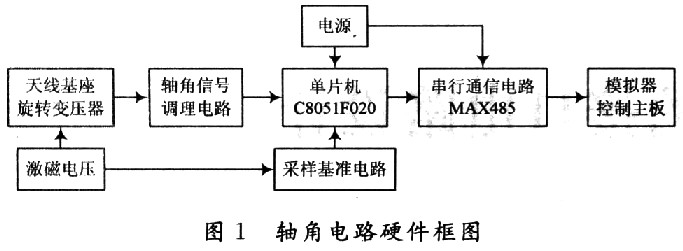
1.1 Antenna shaft angle circuit design The function of the antenna azimuth angle and high-low angle conversion circuit is to convert the analog angle information of the radar antenna into digital angle information, and transmit the digital angle information to the simulator control main board. The main board according to the radar antenna angle The information determines the range of the echo beam and the antenna gain of the target echo.
The conversion of radar antenna angle information is realized by a resolver-digital converter. The hardware circuit takes the single chip microcomputer as the core, including the antenna axis angle conditioning circuit, the reference signal forming circuit and the serial communication circuit. The circuit block diagram is shown in Figure 1.
The signal output from the resolver is generally an AC signal. Taking a certain type of radar as an example, the resolver outputs an AC voltage signal with an amplitude of about ± 10 V. Because the range of ADC conversion analog voltage of the single chip microcomputer (C8051F020) used in the circuit is 0 ~ VRFE (VRFE = 2.45 V), so before the A / D conversion, the analog signal must first be reduced and de-negative value processing, These tasks are completed by the shaft angle signal conditioning circuit, as shown in Figure 2. After the input shaft angle signal undergoes the effect of resistance voltage division and the negative threshold voltage of the diode, the signal that meets the needs of the single chip is output through the resistance voltage division.
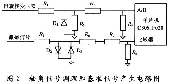
The excitation voltage of the resolver is used as the trigger signal for peak sampling. Because the amplitude of the excitation voltage is greater than the drive voltage of the internal comparator of the single-chip microcomputer, the amplitude limit of the diode is used to form the excitation voltage signal into an approximate square wave signal, and then the resistor is used to divide the signal to ensure that the sampling trigger signal can withstand the comparator In the external driving voltage range (-0.25 ~ + 0.25 V), the circuit is shown in Figure 2. The excitation signal generates the reference signal under the action of the reference signal forming circuit and sends it to the entrance of the comparator of the single-chip microcomputer. The comparator generates an interrupt at the rising edge of the reference signal, enables the A / D port of the single-chip microcomputer during the interruption, and adjusts the signal conditioning circuit of the shaft angle. The antenna azimuth signal is converted into a digital signal. Under the control of the entire single-chip microcomputer program, the circuit completes the digitization of the angle information of the radar antenna and transmits it to the simulator control board through the serial communication circuit.
1.2 Radar main pulse signal acquisition circuit The timing control system in the radar system provides all the timing signals and various control signals required for the normal operation of the radar. The radar main pulse signal is formed by the repetition frequency control circuit of the system and is used as a radar External synchronization signal during debugging of the main station and each sub-system.
The program design of the control board of the simulator uses the radar main pulse as the time reference for the calculation and transmission of the echo data, so as to ensure the synchronization with the radar timing. The specific implementation method is to configure a bidirectional programmable flag pin of the main control chip of the control board as the input mode and the interrupt generation mode, connect to the output end of the main pulse acquisition circuit, and set it to the rising edge interrupt mode. This pin generates an interrupt immediately after receiving the rising edge of the radar main pulse signal. When it is judged that there is an interrupt, the program calculates and sends the radar echo data.
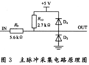
Because the radar main pulse amplitude is a negative pulse signal of about -10 V, and the withstand voltage of the I / O port of the control board is about 3.3 V, so the radar main pulse is used as the time reference for echo generation to the motherboard setting Before the pin, signal conditioning must be performed to achieve the amplitude reduction process. The conditioning circuit designed for the radar main pulse signal is shown in Figure 3. When the input voltage is around OV, the diodes D4 and D5 are cut off, and the output voltage is the partial voltage of the resistors R9 and R10 to the 5 V power supply, which is about 3.3 V. When the input voltage is -10 V, the diode D5 is turned on, and the output voltage is the threshold voltage of the diode D5, which is about -O. 7 V.
1.3 Radar cone sweep reference signal acquisition circuit The magnetic coupling ring rotates synchronously with the reference voltage generator driven by the cone sweep motor, coupling the magnetic field in the circular waveguide to form a high-frequency modulation difference signal. When the radar automatically tracks the target, if the antenna axis deviates from the target direction, an error signal will be generated. The error signal is an AC signal whose frequency is the same as the low-frequency modulation frequency of the feeder system. The cone-sweep reference signal output by the reference voltage generator is also used as the voltage reference of the phase-sensitive detector to detect the error signal. The detected angular error voltage drives the motor to drive the antenna to track the target movement.
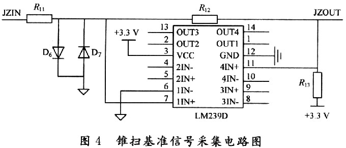
During the actual operation of the radar, the target echo may be received at any time. Therefore, to simulate the radar composite difference signal â–³, it is necessary to determine the phase of each echo relative to the cone sweep reference signal. The phase zero time of the coupling loop is taken out by designing the cone sweep reference signal acquisition circuit, and the phase of each echo relative to the cone sweep reference signal is determined accordingly. The schematic diagram of the cone sweep reference signal acquisition circuit is shown in Figure 4. The circuit uses a voltage comparator chip LM239D, a 3.3 V power supply, and uses a diode to limit the amplitude of the input cone sweep reference signal. The output of the circuit is a 3.3 V square wave signal with the same period as the input signal. It is considered that the rising edge of the square wave is the phase zero point of the cone sweep reference signal. The square wave signal output from the cone-sweep reference signal acquisition circuit is connected to the timer 0 of the control board, set it as an input pin, and uses its pulse width count and capture mode to count the square wave signal.
1.4 Acquisition circuit of radar transmitter working frequency The radar simulator control board is modeled according to the target model, motion law set by the host computer and the complex electromagnetic environment in which the radar is located, and the echo signal of the video segment is calculated in real time. The signal is digitally up-converted to obtain two radar echo signals in the middle frequency band, and then modulated by the radio frequency component to the radio frequency band, and then radiated out through the antenna. Because the analog echo signal finally generated by the radar simulator is in the radio frequency band, the RF component needs to consider the series of processes that the radar actually transmits and receives during design to ensure that the generated analog echo signal is within the radar receiver bandwidth, and It can be changed with the change of radar frequency hopping combination frequency, and the working frequency of the radar at every moment can be displayed on the upper computer display system.
In order to achieve anti-interference, radar usually has multiple operating frequency points, and the control of the operating frequency and change mode of the radar is realized by a frequency hopping control system. The frequency hopping control system works under the comprehensive control of frequency hopping control pulses and control buttons on the system panel, outputs the code of the currently specified frequency to the receiver, and adjusts the operating voltage of the voltage controlled oscillator (VCO) component accordingly to change the VCO Output frequency, which also changes the operating frequency of the radar.
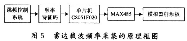
The frequency value corresponding to the operating frequency point of the radar is fixed, as long as the frequency code output by the current frequency hopping control system can be known, the current operating frequency of the radar can be known. The circuit can be designed to determine the current operating frequency of the radar by directly collecting the code of the frequency point. The acquisition circuit uses the single chip microcomputer used in the antenna azimuth signal conversion circuit to control. Because the frequency point characteristic code is a digital signal, it can be directly connected to the digital I / O pin of the single chip microcomputer. The frequency point characteristic code is transmitted to the simulator's radio frequency component through the single-chip microcomputer to control the output frequency of the oscillator. The circuit block diagram is shown in Figure 5.
1.5 Interface serial communication circuit The antenna data information and carrier frequency information collected by the interface circuit are transmitted to the simulator control board through the serial communication circuit. Considering that the situation when the radar simulator is actually working may be far away from the radar, this circuit uses the RS 485 interface bus. The bus uses differential signal transmission, which can effectively suppress the noise interference in long-distance transmission. The maximum transmission distance can reach 1.2 km, and the transmission speed is also fast, which can be as high as 10 Mb / s.
2 Interface circuit performance analysis Integrate the above four signal acquisition circuits on the same interface circuit board. After conducting experimental tests on a certain type of fire control radar, after analyzing the collected radar signals, it can be concluded that the digitizer can complete the digitization of the angle information of the antenna, and the error statistics can be obtained that the angle conversion error is not greater than 1 mil. The main pulse signal of the radar achieves amplitude limiting and voltage reduction through acquisition and conditioning. It provides a trigger pulse for the calculation and transmission of the echo signal of the simulator, and also provides a time reference for echo delay time control and target signal simulation. Due to the large amplitude of the main pulse signal, it will bring some interference to the entire interface circuit. The radar cone scan reference signal can be known as a sine wave after being detected by an oscilloscope, and then converted into a square wave signal with the same frequency through a zero comparison circuit. Using the rising edge of the square wave signal as the phase zero time of the cone scan reference signal, the echo signal can be accurately obtained The phase difference relative to the cone sweep reference signal. For the radar carrier frequency, because the number of radar operating frequency points and frequency values ​​are fixed, as long as the frequency code is collected, the operating frequency can be accurately located, and for different radars, the actual frequency corresponding to the same frequency point code corresponds to The values ​​may be different, so the specific frequency value corresponding to the code of each frequency point of the radar needs to be tested and input into the main control board before the simulator is used.
3 Conclusion Based on the analysis of the above radar signal performance, the interface circuit between the simulator and the radar is designed. The interface circuit has a simple structure and is easy to operate. It is experimentally measured that the signal conversion of the interface circuit is correct and the isolation effect is good. It not only achieves accurate and real-time collection of radar status information, but also does not affect the normal operation of the radar. By comparing the characteristics of different radar working systems and signal characteristics, a unified universal radar interface circuit design can be realized on the basis of the interface circuit design.
Led Ceiling Lamp,Modern Ceiling Lamps,Led Recessed Ceiling Lights,Remote Control Ceiling Lights
Changxing Fanya Lighting Co.,Ltd , https://www.fyledlights.com