Hi3510 is a video compression chip based on the H.264 BP algorithm launched by HiSilicon. The chip uses a multi-core highly integrated SoC architecture with ARM + DSP + hardware acceleration engine and has powerful video processing functions. It can realize the real-time encoding performance of DVD picture quality, and can adapt to various network environments to ensure the clarity and real-time of the picture. The low bit rate H.264 encoding technology greatly reduces the network storage space, and through the integration of DES / 3DES plus The decryption hardware engine ensures network security. Hi3510 adopts 0.13μm technology, LFBGA400 package, size is 19 × 19mm, pin pitch is 0.8mm, integrated on-chip interface including digital video interface, USB, ETH, I2S, I2C, GPIO, SPI, UART, SDRAM, DDR, etc. It can greatly reduce the BOM cost of the device while meeting the development of the device in various application scenarios.
The working principle of Hi3510: The video input unit receives the digital video information output by VADC through the ITU-R BT.601 / 656 interface, and writes the received original image to external memory (SDR SDRAM or DDR SDRAM) through the AHB bus ; Video codec reads images from external memory, performs motion estimation (inter prediction), intra prediction, DCT transform, quantization, entropy coding (CAVLC + Exp-Golomb), IDCT transform, inverse quantization, motion compensation, etc. Operation, and finally write the raw code stream and the encoded reconstructed frame (as the reference frame of the next frame) conforming to the H.264 protocol to the external memory; the video output unit reads the image from the external memory and passes the ITU-R BT The .601 / 656 interface is sent to VDAC for display. The application requirements are different. The image content read by the video output unit from the external storage is also different. When the input image needs to be previewed, the video output unit reads the original from the external storage. Image, when you need to observe the encoding effect of the video encoder, the video output unit reads the encoded reconstruction frame from the external memory; ARM encapsulates the code stream output from the video encoder by the protocol stack and sends it to the network port to achieve Video on demand service.
As shown in Figure 1, the chip is composed of the core of ARM + DSP + video codec accelerator + graphics engine scaler, integrated with rich peripheral interfaces, and internal integration includes such as digital watermarking, DES / 3DES algorithm, so that a single chip can adapt to basic All the work reduces the development difficulty of cooperating with other chips, and eliminates the need for manufacturers to repeatedly develop algorithms and other standard content, which greatly reduces the investment threshold of equipment manufacturers. With the development kits of different application forms of HiSilicon, various products such as PMP, videophone, network monitoring, PVR, and video intercom can be developed.
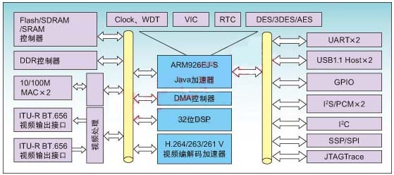
Figure 1: Hi3510 H.264 audio and video codec SoC logic block diagram.
Implementation of Hi3510 codec scheme
As a codec chip for SoC architecture, Hi3510 fully considers compatibility and ease of use when designing. Support almost all series of AD / DA chips produced by the company. Hi3510 can work either as an independent encoder, as an independent decoder, or as a codec at the same time, fully considering the various applications in the codec market. Hi3510 is a typical multi-application single-chip solution, which greatly reduces the BOM composition and cost of the device. Figure 2 shows the application of chip simultaneous encoding and decoding.

Figure 2: Hi3510 is a typical multi-application single-chip solution.
i3510 codec application
Hi3510's own Linux operating system (supports Vxworks, WinCE and other open operating systems at the same time) and ARM processors, in addition to the codec function of the chip, can also realize the development of many rich application functions. As shown in Fig. 2, as long as an ordinary AD is added, the functions of digitization, compression, storage and transmission of composite video signals can be realized. The Hi3510 development kit provides an upper API interface, you can call to implement all chip functions, and can develop your own personalized functions. Figure 3 shows the application design of the chip's coding scheme.
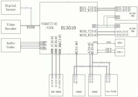
Figure 3: Application design of Hi3510 chip coding scheme.
The decoder application is the same as the encoder in the architectural design (convenient solution can maintain consistency, can realize a set of hardware to meet unsatisfactory requirements, only need software upgrade). The decoder only needs to be equipped with a DA chip (if the LCD digital screen can save this chip), it can realize the function of decoding the data stream, and realize the user-machine interactive menu operation through the GUI or OSD, to achieve PMP and other similar functions. Applications. Figure 4 shows the application design of the chip's decoding scheme.
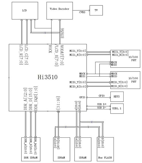
Figure 4: Application design of Hi3510 chip decoding scheme.
Summary of this article
The application of H.264 standard provides technical support for the network transmission of video, especially the transmission under low bandwidth (such as wireless transmission mode). In today's explosion of information, the market requires designers to launch products faster and faster, and in order to maintain the competitiveness of products, product prices and product application features must maintain sufficient advantages, especially in the multimedia market. On the basis of providing standard algorithms, Hisilicon ’s SoC chip gives designers maximum flexibility to design suitable products, greatly reducing the manufacturer ’s input costs, shortening the time for manufacturers to launch new products, and preparing for winning the market .
Introduction of Inverter Filter
Rated currents: 6 to 2000A
Stud or terminal block optional (above 250A it is copper bar)
FT330/FT330T series are general purpose filters, suitable for most inverter brands
Could be customized according to the real interference of customer`s working field
Features of Inverter Output Filter
FT330 series is designed according to the frequency characteristics of interference generated by inverter when it works towards power grid or other digital equipment.
Three-stage filtering design, high impedance at broad frequency range due to special magnetic materials adopted.
Assure the smooth operation of other electronic devices in the vicinity, solve the interference problems of inverter;
FT330T series is specially designed according to the frequency characteristics of interference generated by inverter output when it works towards load;
Effectively solve abnormal conditions such as load heating and howling that are easy to occur during long-distance transmission of frequency inverters, and better effect can be achieved with reactors;
Effectively control the common mode interference along the cable to protect load and increase its service life;
Touch-safe terminal block versions are available to meet the high safety requirement of certain special applications;
Copper bar terminals applied for versions above 250A to keep pace with international standard, easy and safe connection;
Optional 520VAC/690VAC (and above) high voltage versions.

Inverter Filter
Inverter Filter,Inverter Output Filter,Inverter RFI Filter,Power Inverter Noise Filter
Jinan Filtemc Electronic Equipment Co., Ltd. , https://www.chinaemifilter.com