|

While maintaining the dynamic range of the original signal, the headphone output of the notebook PC must drive a low-impedance load with a signal amplitude of 1Vrms (typical value is 32Ω; sometimes as low as 16Ω). This task seems simple, but further analysis will reveal that it faces some harsh realities: When powered by a single power supply, the headphone output must maintain the dynamic range, and the power supply voltage is usually obtained from the DC-DC converter, and the high-speed digital Circuit sharing. Based on the signal amplitude and load impedance of these circuits, the peak current drawn from the power supply can reach 90 mA. When the power supply or headphone driver is turned off, clicks and transient noises should not be heard. Power supply noise In order to achieve a reasonable signal-to-noise ratio, the influence of power supply noise on the output of the headphone amplifier must be suppressed, and the power supply suppression of the headphone driver is the key to reducing the signal-to-noise ratio. For example, the dynamic range based on CD or DVD signals may exceed 90dB. Assuming that there is 100mV noise on the audio power supply voltage, most of its spectral components are within the audio bandwidth. In order to maintain the 90dB dynamic range, the noise output from the headphones must be reduced to about 30µV. To achieve this, the PSRR of the headphone driver must exceed 70dB at the frequency of interest.
To obtain the above power supply rejection ratio in the audio frequency band, a well-thought-out design scheme must be adopted so that the amplifier can provide a certain suppression ability to the power supply noise in the audio frequency range. After browsing the data of most op amps, you will find that PSRR is usually higher near DC, and as the frequency increases, it will drop sharply (usually -20dB / ten octave). At 20kHz, the PSRR of some devices is below 40dB.
Some DC-DC converters produce higher noise content at the upper end of the audio spectrum. Although it can be confirmed that there are few audible components at those frequencies, noise can still be measured at the output of the headphones. Please note that for the audio DAC (or CODEC) with built-in headphone driver, most of the data will not attract readers' attention to the PSRR indicator. Even if it is mentioned, it usually appears as an entry in the electrical characteristics without giving a PSRR vs. frequency curve.
Since most headphone amplifiers cannot provide enough PSRR, an external low voltage regulator (LDO) can be added to purify the headphone amplifier's power supply. For example, in order to obtain a sufficient power supply noise suppression ratio at the audio output terminal of a notebook PC, where + 5V is still the general audio circuit power supply voltage, and a specific node is usually adjusted to about 4.7V.
ICs like the MAX4298 / MAX4299 (ultra-high PSRR stereo driver) improve PSRR by fine-tuning internal key nodes inside the device, much higher than those obtained by other methods. This method makes the PSRR at 1kHz exceed 100dB, eliminating the need for an external voltage regulator (Figure 1).
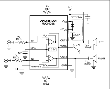
Figure 1. In a typical MAX4298 application, please note that the 220μF AC coupling capacitor blocks the DC voltage of the headset. Optional components are used to control the magnitude of power-off transients. Noise suppression Noise suppression is another measure of IC capability, that is, the ability to minimize sudden noise or panic transient noise that occurs when the IC is muted or powered on (or powered off). It is difficult to obtain such performance in the output driver, because for the output driver, there is no downstream circuit that can be muted, thereby shielding the occurrence of abnormal signals. If headphones are plugged in, no matter what driver is used, it will inevitably cause transient performance of the audio system.
The headphone driver is usually powered by a single power supply, and realizes AC coupling to the output of the plug hole through a large capacitor, as shown in FIG. 2. Such an arrangement can prevent a DC voltage from appearing across the earphone, which may damage the driving unit of the earphone. During operation, since the headphone side of the capacitor is ground potential, and the amplifier output bias is about half of the full swing, there is voltage across the DC blocking capacitor. When the power is turned on, the capacitor must be charged to the operating voltage, but the current flowing through the capacitor must be allowed to flow through the load (headphone audio coil). So what method can be used to prevent the current from generating noise signals?
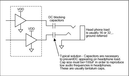
Figure 2. This circuit is a typical configuration for a headphone driver in a single-supply product. It includes a series capacitor, which together with the headphone impedance forms a high-pass filter (necessary for blocking DC from the headphone).
Some designs use the JFET and discrete components around the amplifier output to suppress the charging current, and some circuits provide an RC time constant to slow down the sound transient during turn-on, thereby reducing the interference factor by reducing the content of the interference frequency. Some products use a back-to-back exponential ramp (S-shaped) to further suppress noise caused by power-up. Different from the RC index method, this method of inhibition does not cause dv / dt mutation.
It is difficult to solve the instantaneous change when power is off. How can the amplifier control the discharge of the output capacitor without power? One method is to provide a standby power supply for the headphone amplifier. The power supply is provided by a fully charged capacitor when the power is turned on. After the main power supply is removed, the capacitor can also provide enough energy to gracefully turn off the amplifier. The integrated application of this technology (Figure 1) produces the waveform shown in Figure 3.
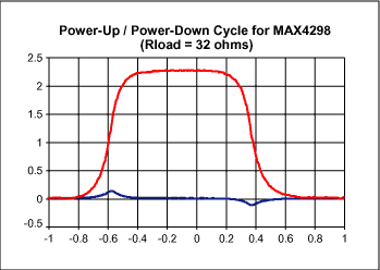
Figure 3. These waveforms illustrate the effect on the circuit shown in Figure 1 when VCC is turned on (t = -1s) and VCC is removed (t = 0s). VCC is not given here. Please note that the S-shaped transition at the output of the MAX4298 (upper curve) produces a smooth and limited output interference (lower curve) at the load. The controlled output limits the sound transients at turn-on to a lower level, and the human ear is less sensitive to them.
As shown in Figure 3, additional components are used to control the sound transient when the MAX4298 is powered off, suppressing transient noise at power-up. This technique involves the use of the auxiliary VCC pin (SVCC). When VCC is provided, the external Schottky diode charges the energy storage capacitor. When the power supply is removed, the working process of the MAX4298 is as follows: Audio mute. The stereo amplifier reverts to low transient current mode and draws power from the SVCC pin. The output bias voltage slowly changes to ground, and the power-on transient is suppressed by mirroring the power-on waveform and the S-shaped mode is used to eliminate the dV / dt mutation. The energy storage capacitor is discharged, because the output voltage is ground, so when the SVCC power supply finally disappears, the transient of the output audio can be ignored. Distinctive methods In order to achieve an unclear index, the above scheme requires considerable effort (additional lines need to be added to the BOM), and the market will not evaluate this feature very high. The ideal method is to completely eliminate the output capacitor, thereby eliminating the effects of charging or discharging through the audio coil of the headset. These capacitors can be eliminated by providing DC coupling for the headphone drive, 0V output bias, and powering the amplifier with a bipolar power supply.
Even though most battery-powered designs are limited by single-ended power supplies, designers have some options. One option is to use a third amplifier to provide the headset with half the full swing offset, which creates a "pseudo 0V" output offset. Since the bias of the main stereo amplifier is also half of the full swing, the DC coupling capacitor can be omitted. Therefore, the third amplifier must have the ability to draw and supply current from the two main amplifiers and be sufficient to handle ESD discharge when any headphone plug (plug hole must be isolated from the chassis) is inserted.
Another option is to use the provided positive power supply to generate a dedicated negative power supply, or use a traditional negative power generating device (Figure 4). For this method, ESD and grounding are not a problem, and the additional voltage amplitude almost doubles the peak-to-peak output voltage-this is useful when using a + 3V or less + 3V power supply.
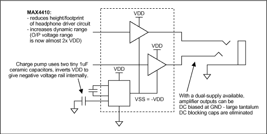
Figure 4. To achieve dual power supply for the amplifier, the on-board charge pump inverts the positive supply voltage. Series capacitors are no longer needed, but small ceramic capacitors need to be provided for the charge pump. The use of ceramic capacitors reduces the area of ​​the PCB.
The MAX4410 headphone amplifier generates an internal negative power supply through the positive power supply pin. Since the DC output of the amplifier is biased at 0V, no output capacitor is required. The internal lockout circuit prevents spurious operation caused by too low or power supply voltage during power-on and power-off, so there is no noise. Because the output voltage swing of the amplifier is almost twice that of a single supply voltage, other advantages can also be obtained, including a larger signal swing and greater output power. Further obstacles The current ongoing design usually makes many compromises before the product is put on the market. For example, ESD requirements may require magnetic beads or other EMC measures between the headphone driver and the plug hole. These components may constitute a large impedance in the audio frequency range, which may cause crosstalk problems and output power loss. However, careful design and Kelvin measurement technology can reproduce good audio performance.
Headphone return current also needs to be considered. When the current is increased to 100mA, the limited impedance on the ground plane or PCB leads may produce a significant IR drop. A similar mechanism makes the SNR worse when it is shared with the DC-DC converter. To solve similar problems, it may be helpful to use special return leads or copper. The digital future? Unless digital input headphones develop rapidly, the circuit that drives the headphone jack still requires analog circuits. Class D design can maintain the performance of the digital audio path up to the output of the amplifier, although filter components are required to maintain efficiency and reduce EMI. PSRR and noise suppression will still affect system performance, so for a long period of time, analog hardware design is still of great significance.
Scope of supply
SCOTECH`s oil immersed distribution transformers Including single phase distribution transformer, Three Phase Distribution Transformer, Pole Mounted Transformer, Pad Mounted Transformer, miniature substation and amorphous metal transformer.
small size Distribution Transformer: up to 315KVA
medium size distribution transformer: up to 2500KVA
large size distribution transformer: up to 25MVA
Standards
SCOTECH`s oil immersed distribution transformers are designed and manufactured in accordance with all major international standards (IEC, ANSI, UL, etc.)
Applications
Power grid, lighting, utility, industrial and others.
Why SCOTECH
Long history- Focus on transformer manufacturing since 1934.
Technical support – 134 engineers stand by for you 24/7.
Manufacturing-advanced production and testing equipment, strict QA system.
Perfect service-The complete customer service package (from quotation to energization).
Distribution Transformer
Distribution Transformer,Electrical Distribution Transformer,Oil Cooled Distribution Transformer,Pole Mounted Distribution Transformer
Jiangshan Scotech Electrical Co.,Ltd , https://www.scotech.com