1 Introduction
FPGA (Field Programmable Gate Array) field programmable gate array is further developed on the basis of PAL, GAL, PLD. As a semi-custom circuit in the field of application specific integrated circuit (ASIC), FPGA not only solves the custom circuit. Insufficient, and overcome the shortcomings of the limited number of original programmable device gates. Using FPGAs to develop digital circuits can dramatically reduce design time. From simple NAND gates to high-performance CPUs, FPGAs can do all digital devices.
2 software platform builder
When designing an FPGA embedded system, it is often necessary to access peripheral devices such as LEDs and audio interfaces through software programming. Touch screen, etc. However, you need to be familiar with the working conditions of the relevant peripherals when programming, including the device registers required for the device to work. Device specific commands. The communication protocol used and the interrupts that need to be processed. The software platform builder (SPB) of the AD software provides the underlying modules (software IP modules) associated with configuration data and drivers for these specific peripherals, providing an application programming interface (API) for accessing peripheral devices.
When designing an embedded system under AD software, the use of SPB is implemented through a software platform file (SwPlatform). SPB is a graphical user interface that can read the FPGA design by itself, import the appropriate low-level modules for the peripheral devices in the design, and add more high-level IP modules to the software platform files based on this. Which IP module is specifically added depends on which peripheral devices need to be accessed in the FPGA embedded design. When accessing peripheral devices, you can use multiple IP modules provided by SPB. The lower-level IP module can access a specific storage device, such as a hard disk. SD card. RAM drives, higher-level IP blocks are more abstract and more hardware-independent.
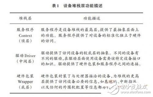
The software platform file (SwPlatform) is a software layer selected from a series of provided components in the SPB. Software platform files enable applications to leverage hardware, such as storage services and network services, through a standardized set of services. The purpose of the software platform file is to enable the hardware device to provide an application programming interface (API) for the peripheral device through an abstract and common software interface. The Device Stacks in the software platform consists of three types of modules, each of which is a hardware wrapper. Driver and Con-text. The device stack is typically built from the bottom up, starting with the lowest-level modules associated with a particular hardware device on the schematic design. On top of this, higher-level modules can be stacked, providing a more general function of accessing peripherals. At the bottom of the device stack is the hardware wrapper, then the driver, and finally the Context. The higher the level of abstraction of the module to the hardware, the higher the stack. The function description of the device stack layer is shown in Table 1.
The Software Service in SPB is a type of application that can be used by an application. definition. Structure and function functions. The software service is included to access the SD card. IDE storage device. Storage services for files on CF cards and flash memory; network services for providing Ethernet access; core services that provide POSIX-compliant multi-threading capabilities; GUI services that allow rapid construction of modern graphical interfaces; for audio and video functions Multimedia service. System services for interrupt management and software timing management are always present in the software platform and are independent of specific devices. Each different software module contains complete API reference information. API reference information can be accessed through the API Reference, and each layer in the stack has a detailed description of the functions available on that layer. View Header 2 embedded audio processing system design for any driver or service program with Header Files
2.1 OpenBus system design
In the embedded design, when dealing with the connection relationship between the peripheral device and the processor, the open bus (OpenBus system) in the AD software can be used, so that the connection process will be greatly simplified. The "OpenBus System" is a term describing a "module" connection that uses a common bus to implement logical functionalities throughout the system [3]. In the OpenBus system documentation, open the OpenBus Palette panel and select and place the components needed to make up the system. Devices used in FPGA design in the OpenBus Palette panel are classified as Connectors by function. Processors. Memories. Peripherals (peripherals), etc. Each OpenBus device must be properly configured before it can be used. This Open-Bus system is designed differently than traditionally placing the processor and peripheral circuitry as components on the board. It removes all low-level traces and interconnect details and allows the system to be built quickly.
In the embedded audio processing system of this paper, the audio stream signal is obtained by accessing the high-fidelity audio interface on the NB3000 development board. In the design of the OpenBus main processor system, select and place the microprocessor (32-bit RISC Processor TSK3000A). Connector (Interconnect). I2S Audio Streaming Controller (Audio Streaming Control-ler). OpenBus devices such as SPI controller (SPI Controller) and SRAM controller (SRAMController) are connected as shown in Figure 1. At the same time, parameters are configured for the OpenBus device. Configure the data transfer size parameter of the SPI controller to 32. Configure the I2S Hardware Buffer parameter of the I2S audio stream controller as 4k samples and I2S to the interrupt number INT_I1.
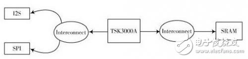
Figure 1 OpenBus system design
In general, any FPGA design that uses the OpenBus system must design a top-level schematic that places the interface circuitry. The Open-Bus system file in Figure 1 acquires audio stream data for the 32-bit processor TSK3000A and I/O interface logic, including the host processor system in the FPGA design. The constraint file connects the port at the top of the schematic to the actual physical pin of the target FPGA device. The constraint file contains not only port-to-pin mapping, but also clock distribution. Other relevant design specifications such as target devices.
The top-level schematic connects the embedded system design downloaded to the FPGA to the physical pins of the FPGA device through a constraint file. In the top schematic design, the audio stream controller I2S is connected to the audio codec (AUDIO_CODEC), and the SPI controller is connected to the audio codec controller CS4270 (AUDIO_CODEC_CTRL), as shown in Figure 2.
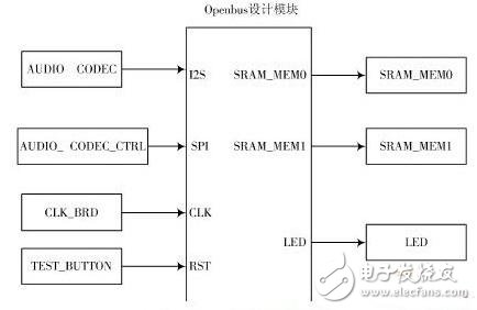
Figure 2 Top-level schematic design
2.2 software platform file design
On the basis of SPB, build a software platform file (SwPlat-form) that accesses the audio interface of the NB 3000 development board and processes the audio stream data, as shown in Figure 3.
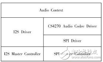
Figure 3 Software block diagram of the software platform builder
8 Layer PCB - Stackup & Cost & Prototype manufacture
What is 8 layer PCB?
The 8 layer PCB is a circuit board with 8 layers that are stacked firmly together with predefined and dependable mutual connections between the layers. Structure of eight layer PCB is more complicated. Nowadays, PCBs frequently have 8 to 12 layers or more, and electronics engineers know that designing for so many layers requires a well-configured layer stack.
8-layer Printed Circuit Boards are usually installed in compact equipment with strict spacing requirements, such as notebook computer motherboard, communication backplane, wearable watches, etc. Because of its complexity and high manufacturing costs, your 8-layer PCB Manufacturing should be made by reliable and experienced manufacturers. Jinghongyi PCB has been specially targeting high-end PCB manufacturing and assembly services for 8 years, providing high-quality products and services for various customers. Our advanced production line and fast response team will keep you comfortable and reassured, without any trouble, you can rest assured to place the order with us.

Typical 8-layer PCB stack up methods and guidelines
Standard stackup of 8 layer PCB looks as follows
- Signal1
- Ground
- Signal2
- Power
- Ground
- Signal3
- Power
- Signal4
Eight-layer PCB can be used to add two additional layers, or two planes can be added to improve EMC performance. Most eight-layer circuit boards are superimposed to improve EMC performance, rather than adding additional wiring layers. Compared with 6-layer circuit boards, the cost increase percentage of 8-layer PCB is less than that of 4-layer PCB to 6-layer PCB. Therefore, in order to improve EMC performance, the cost increase is reasonable. Therefore, most 8-layer boards consist of four wiring layers and four planes.

8 Layer PCB Stack up

8 Layer PCB stackup
In short, 8 layer PCB are usually used to improve the EMC performance of circuit boards, rather than increasing the number of layers.
No matter how you decide on the stack layer, it is not recommended to use an 8-layer PCB Board with six wiring layers. If you need six routing layers, you should use a 10 Layer PCB board. Therefore, the 8-layer board can be regarded as the six-layer board with the best EMC performance.
Basic Layer of Eight-Layer Circuit Board with Excellent EMC Performance

All signal layers are adjacent to the plane, and all layers are tightly coupled. High-speed signals are buried between planes, so planes provide shielding to reduce the transmission of these signals. In addition, the circuit board uses multiple grounding layers to reduce the grounding impedance.
Other forms of 8-layer PCB stackup

A typical 8 Layer PCB Stackup

0.062[8 layer PCB stackup

0.093[ 8-Layer PCB Stackup
So far, we have also clarified the cost and price differences between 6-layer PCB, 8-layer PCB and 10-layer PCB.
8 Layer PCB thickness

8 LAYER 1.6 MM STANDARD STACKUP AND THICKNESS
8 Layer Stackup - 1.6mm thickness |
||||||
| layer order | layer name | material type | material description | dielectric constant | thickness | copper weight |
| 1 | top | copper | signal | 0.035mm | 1 oz | |
| 2116 | prepreg | 4.5 | 0.12mm | |||
| 2 | inner 1 | copper | plane | 1 oz | ||
| core | 4.6 | 0.3mm | ||||
| 3 | inner 2 | copper | plane | 1 oz | ||
| 7630 | prepreg | 4.7 | 0.2mm | |||
| 4 | inner 3 | copper | plane | 1 oz | ||
| core | 4.6 | 0.3mm | ||||
| 5 | inner 4 | copper | plane | 1 oz | ||
| 7630 | prepreg | 4.7 | 0.2mm | |||
| 6 | inner 5 | copper | plane | 1 oz | ||
| core | 4.6 | 0.3mm | ||||
| 7 | inner 5 | copper | plane | 1 oz | ||
| 2116 | prepreg | 4.5 | 0.12mm | |||
| 8 | bottom | copper | signal | 0.035mm | 1 oz | |
| Final board thickness: 1.6mm±0.13mm | ||||||
8-Layer Prototype PCB Manufacturing Service
The 8-layer prototype FR-4 PCB is an 8-layer circuit board, which is firmly stacked together with predefined and reliable interconnection between layers. The 8-layer FR-4 PCB has more complex structure. JHYPCB is a large enterprise located in Shenzhen, China, which can manufacture 8-layer prototype PCB.
JHYPCB can provide you with multi-layer PCB board in accordance with RoHS standard. With laminated material, it can match high temperature in assembly process. Importantly, some lead-free assembly processes will require laminated substrates to withstand temperatures exceeding 260 degrees Celsius or 500 degrees Fahrenheit over a longer period of time. To solve this problem, we have high temperature laminates in stock, so that our customers can meet the higher temperature cycle requirements of some lead-free assembly applications.
JHYPCB is one of the leading 8 layer PCB manufacturers. For more information, pls send email to us.

8 Layer PCB
PCB Circuit Board,8 Layer PCB,Custom multilayer pcb,Custom 8 Layer PCB
JingHongYi PCB (HK) Co., Limited , https://www.pcbjhy.com