0 Preface
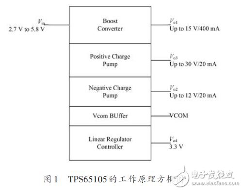
The TPS65105 is a hybrid DC/DC converter integrated circuit chip. Designed to power thin-film transistor (TFT) LCD displays, the LCD requires three output voltages. The chip's internal auxiliary linear regulator provides a 3.3 V bus supply voltage output from the 5 V input supply for the power supply system.
Its internal main output Vol is a fixed frequency PWM step-up DC/DC transformer operating at up to 1.6 MHz, which provides a supply voltage to the drive source of the LCD display. The chip also integrates a DC/DC converter controller with different power switch current limits. The TPS65105's power switch current limit is typically 2.3A. The integrated charge pump integrated into the chip can be used to provide an output voltage of 2x/3x for the LCD positive gate driver. A negative charge pump controller is also provided internally to provide a negative voltage output to the LCD negative gate driver. Since the charge pump's switching frequency is as high as 1.6 MHz, the charge pump capacitor used can use a lower cost, smaller 220 nF capacitor. The family integrates a VCOM buffer to provide power to the LCD backlight, a linear regulator controller that provides an 3.3 V output voltage to the digital circuitry using an external crystal Power Transistor. For absolute safe and reliable operation, the series also has output over-current, over-temperature and short-circuit protection functions, that is, when any output of the chip is overcurrent, overheated or short-circuited, it will enter the shutdown mode. The series also features off-mode external control, soft-start and output voltage detection.
1 main performance
(1) The input voltage range is 2.7~5.8 V;
(2) The fixed operating frequency is up to 1.6 MHz;
(3) has three independent output voltages;
(4) The main output voltage can be as high as 15 V, and the accuracy can be as high as 1% or more;
(5) The negative output voltage is -12 V/20 mA;
(6) The positive output voltage is 30 V/20 mA;
(7) A VCOM buffer is integrated internally;
(8) Linear regulator controller with 3.3 V auxiliary output;
(9) has a soft start function;
(10) has a power-on sequence control function;
(11) has all output fault detection functions;
(12) With overheat protection.
2 internal principle block diagram
The working principle block diagram of TPS65105 is shown as in Fig. 1.
Fast Recovery Diode (FRD) is a semiconductor diode with good switching characteristics and short reverse recovery time. It is mainly used in switching power supplies, PWM pulse width modulators, inverters and other electronic circuits as high-frequency rectifier diodes. Free-wheeling or damper diodes are used. The internal structure of the fast Recovery Diode is different from that of an ordinary PN junction diode. It belongs to a PIN junction diode, that is, a base region I is added between the P-type silicon material and the N-type silicon material to form a PIN silicon wafer. Since the base area is thin and the reverse recovery charge is small, the fast recovery diode has a short reverse recovery time, a low forward voltage drop, and a high reverse breakdown voltage (withstanding voltage).

Fast Recovery Stud Diode,Stud Type Fast Recovery Diode,Fast Recovery Diode,Stud Rectifier Power Diode
YANGZHOU POSITIONING TECH CO., LTD. , https://www.yzpst.com