Years ago, Beamsky published an article about DDR cabling guidance, which was very popular on the web and was attended by many of its peers. It seems that the article is not well written, the logic is not strong, and the operability is not strong.
In the development of hardware products in recent years, I have summarized a set of DDR wiring methods, which is highly feasible. So I wrote another such article. In addition to the DDR wiring rules, I also want to talk about the wiring process. My wiring process can take a lot of detours. All the methods that will be covered in this article, the wireless era (Beamsky) have been tested.
DDR cabling is usually an important part of hardware product design. It is precisely because of its importance. There are also a lot of people on the network discussing DDR cabling rules. There are many peers who are ignorant of the DDR cabling. I am going to do the opposite and talk about the simplest rules and processes of DDR wiring.
If not specified, the method in each step applies to both DDR1, DDR2 and DDR3. PCB design software uses Cadence Allgro 16.3 as an example.
The first step is to determine the topology (useful only for multiple DDR chips)
First of all, we must determine the topological structure of DDR. In a word, DDR1/2 adopts star structure, and DDR3 adopts daisy chain structure.
The topology structure only affects the routing of the address lines and does not affect the data lines. The following is a schematic diagram.
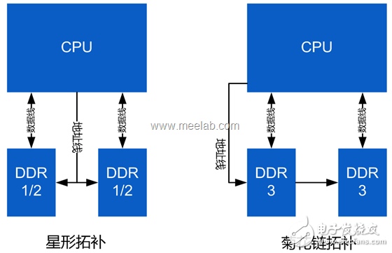
The star topology is that the address line goes to the middle of two DDRs and then the two DDRs are separately routed. The daisy chain uses the address line to "string up" two DDRs, just like a kebab, each DDR is on a kebab. A piece of meat, haha, make a joke.

The second step, the components are placed
Once the DDR topology is determined, components can be placed. There are several principles to follow:
Principle 1, consider the topology, carefully look at the location of the CPU address line, so that the address line is beneficial to the corresponding topology
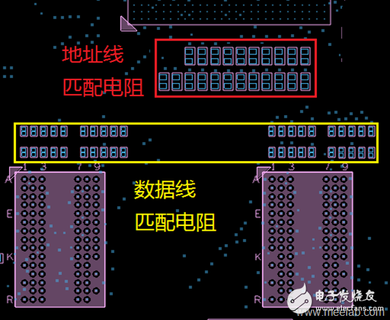
Principle 2, the matching resistor on the address line is close to the CPU
Principle 3, the matching resistor on the data line is close to DDR
Principle 4, placing and rotating the DDR chip, so that the DDR data line is as short as possible, that is, the data pin of the DDR chip is close to the CPU.
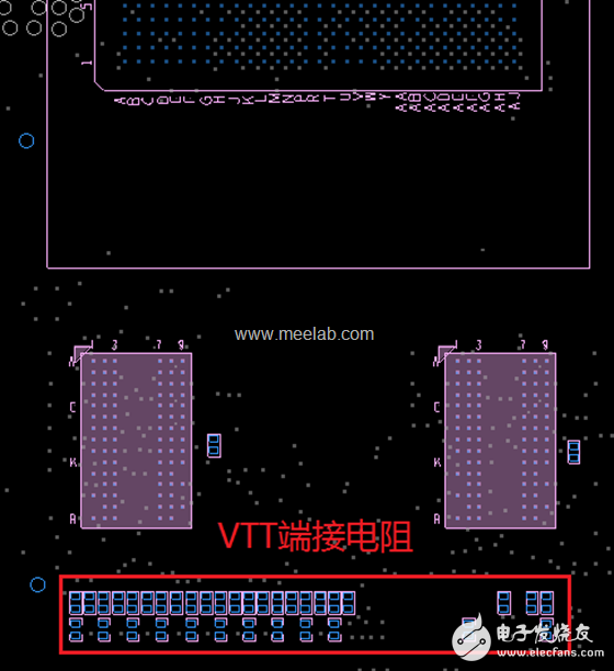
Principle 5, if there is a VTT termination resistor, place it at the farthest position where the address line can go. In general, DDR2 does not require a VTT termination resistor, only a few CPUs are required; DDR3 requires a VTT termination resistor.
Principle 6, the decoupling capacitor of the DDR chip is placed close to the corresponding pin of the DDR chip.
The following is a schematic diagram of the components of DDR2 (not including decoupling capacitors). It can be easily seen that the address line can go to the middle of two chips and then divide to the two sides. It is easy to implement star topology. At the same time, the data line will be very short.
The following is a schematic diagram of the placement of DDR2 components with VTT termination resistors. In this example, there is no series matching resistor, and the VTT termination resistor is placed at the farthest distance that the address line can reach.
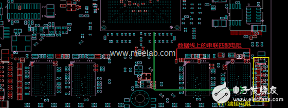
The following is a schematic diagram of DDR3 components placement. Please note that the CPU used here supports dual-channel DDR3, so there are four DDR3s (reference design is 8). In fact, each channel constitutes one channel, and the address line is along the map. In the middle of the green routing, the daisy chain topology is realized.
The VTT termination resistor on the address line is placed furthest away from the address line. Similarly, the termination resistors on the data lines are placed close to the DDR3 chip, and the distance from the data line to the CPU is very short. At the same time, it can be seen that the decoupling capacitor is placed very close to the corresponding power supply pin of DDR3.
The third step is to set up a simulation model of the series matching resistor.
After placing the components, it is recommended to set up a simulation model of the series matching resistors, which is beneficial for the subsequent routing rules.
Click Analyzeïƒ SI/EMI Simïƒ Model Assignment, as shown below.
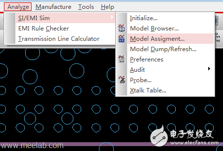
Then the Model Assignment interface will appear, as shown below:

Then click on the device that needs to set up the model, usually a series matching resistor, assign or create a suitable simulation model. If you don't know how to create it, search on the Internet or send an email to the wireless era (Beamsky).

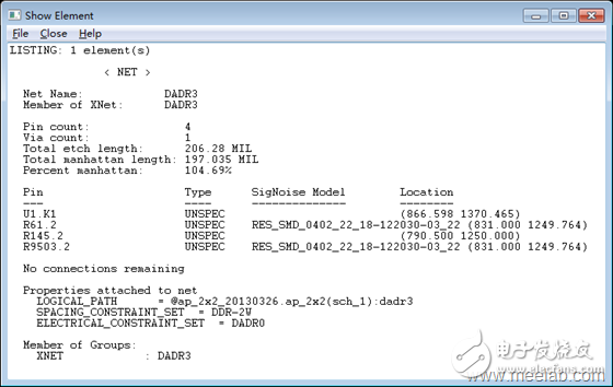
After assigning the network after the simulation model, you can see the related XNET properties by using the Show Element command, as shown below:
The fourth step is to set the line width and line spacing.
1. DDR trace line width is closely related to impedance control. It is often seen that many peers do impedance control. For pure digital circuits, there is a condition for single-ended impedance control for high-speed lines; but for hybrid circuits, including high-speed digital circuits and RF circuits, RF circuits are more important than digital circuits, and 50-ohm impedance control must be performed on RF signals. At the same time, the RF traces may not be too thin, otherwise it will cause a large loss, so in the hybrid circuit, I often abandon the impedance control of the digital circuit. So far, the highest specification DDR in the hybrid circuit product I designed is DDR2-800, which is not controlled by impedance and works normally.
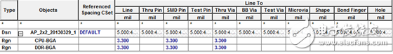
2. DDR power supply routing, recommended more than 8mil, in Allegro can be set for the physical parameters of a class of lines, I personally like to establish PWR-10MIL constraints, and assign this constraint to all power networks, as follows Figure.

3. The line spacing is mainly considered in two aspects. One is the line-to-line spacing. It is recommended to adopt the 2W principle, that is, the line spacing is 2 times the line width, 3W is difficult to meet; the second is the line-Shape spacing, and the 2W principle is also recommended. For line spacing, you can also create a constraint in Allegro that assigns such constraints to all DDR traces (XNET), as shown below:
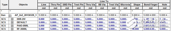
4. Another rule that may be needed is the regional rule. The default line width and line spacing in Allegro is 5mil. When the CPU pins are dense, such a rule cannot be satisfied. This requires setting the area rule that allows small spacing and small line width around the CPU or DDR chip. ,As shown below:
The fifth step, the line
There are a lot of things to pay attention to when you are going to the line. Here is just a little explanation.
Keep all traces as short as possible
The line cannot have an acute angle
Try to make fewer holes
Ensure that all traces have a complete reference plane, either the ground plane or the power plane. For alternating signals, the ground and the power plane are equipotential.
Try to avoid the vias breaking the reference plane, but this is hard to do in practice.
After the address line and data are finished, be sure to remove the power supply pin, grounding pin, decoupling capacitor power supply pin and grounding pin of the DDR chip. Otherwise, it will be troublesome when winding around the same length.
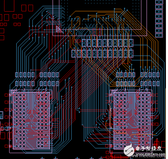
The figure below is the completed DDR trace, but it has not been equal:
The sixth step is to set the equal length rule.
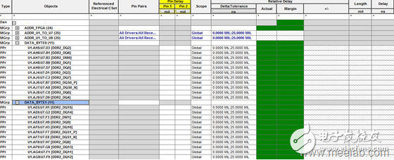
For data lines, the rules for DDR1/2 and DDR3 are the same: each BYTE is as long as its own DQS, DQM, ie DQ0:7 and DQS0, DQM. Isometric, DQ8: 15 is equal to DQS1, DQM1, and so on.
DDR2 data line equal length rule example
DDR3 data line equal length rule example

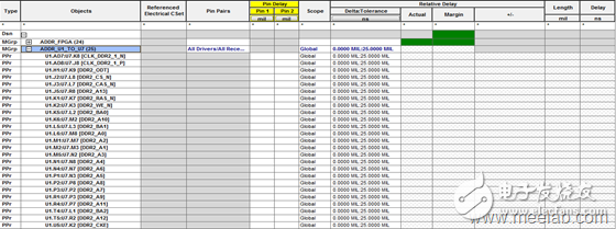
The length of the address line, pay special attention to, DDR1/2 and DDR are very different.
For DDR1/2, you need to set the distance of each address to the same DDR to be the same length, as shown below:
For DDR3, the equal length of the address lines often requires vias to be matched. The specific rules are bound to the vias and the VTT termination resistors, as shown below. It can be seen that the address line of the CPU reaches the via hole by the same length, and the distance from the via hole to the VTT termination resistor is also the same length.

In addition, many times, the length requirements of the address line are not strict, I have not tried this. In the products I designed, the address lines and data lines have been set by the equal length rule of 25mil Relative Propagation Delay. Details about the setting of the equal length rule are not repeated here. If you are interested, you can send an email to the wireless era (Beamsky).
The seventh step, the same length
After completing the setting of the equal length rule, the last step is also the one with the most workload: winding the same length.
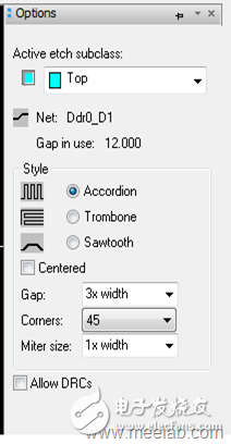
In this step, I think there is only one rule that needs attention: try to use 3 times the line width and 45 degrees to wrap the same length, as shown below:
After the completion of the equal length, it is best to lock the DDR-related network to avoid misoperation.

Here, the DDR cable has been completed. The three or forty products I have designed are completed according to the above rules and procedures. The highest specification of DDR2 is DDR2-800, 512MB, and the highest specification of DDR3 is DDR3. -1600, 1GB, can work very stable, no problem, no matter the performance or reliability.
ZGAR AZ MC Disposable
ZGAR electronic cigarette uses high-tech R&D, food grade disposable pod device and high-quality raw material. All package designs are Original IP. Our designer team is from Hong Kong. We have very high requirements for product quality, flavors taste and packaging design. The E-liquid is imported, materials are food grade, and assembly plant is medical-grade dust-free workshops.
Our products include disposable e-cigarettes, rechargeable e-cigarettes, rechargreable disposable vape pen, and various of flavors of cigarette cartridges. From 600puffs to 5000puffs, ZGAR bar Disposable offer high-tech R&D, E-cigarette improves battery capacity, We offer various of flavors and support customization. And printing designs can be customized. We have our own professional team and competitive quotations for any OEM or ODM works.
We supply OEM rechargeable disposable vape pen,OEM disposable electronic cigarette,ODM disposable vape pen,ODM disposable electronic cigarette,OEM/ODM vape pen e-cigarette,OEM/ODM atomizer device.


Disposable E-cigarette, ODM disposable electronic cigarette, vape pen atomizer , Device E-cig, OEM disposable electronic cigarette
ZGAR INTERNATIONAL TRADING CO., LTD. , https://www.zgarette.com