1 Introduction
In the 21st century, mankind will face major challenges in achieving sustainable economic and social development. Under the dual constraints of limited resources and environmental protection, the energy problem will be more prominent, which is mainly reflected in: 1 energy shortage; 2 environmental pollution; 3 greenhouse effect. Therefore, when solving energy problems and achieving sustainable development, mankind can only rely on scientific and technological progress to develop and utilize renewable and clean energy on a large scale. Solar energy has the advantages of large reserves, ubiquitous existence, economic utilization, clean and environmental protection, etc. Therefore, the utilization of solar energy has been paid more and more attention by people and become an ideal alternative energy source. The power described in the paper is a 200W solar photovoltaic grid-connected inverter, which directly converts the direct current generated by the solar panel into a 220V/50Hz power frequency sinusoidal AC output to the grid.
2 system working principle and its control scheme
2.1 Photovoltaic grid-connected inverter circuit principle
The main circuit schematic diagram of the solar photovoltaic grid-connected inverter is shown in Figure 1. In this system, the solar panel outputs a DC voltage of 62V, which is converted to 400V DC by a DC/DC converter, and then 220V/50Hz AC is obtained after DC/AC inverter. The system ensures that the 220V/50Hz sinusoidal current output by the grid-connected inverter is synchronized with the phase voltage of the grid.
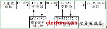
Figure 1 circuit block diagram
2.2 System Control Scheme
2 is a main circuit topology diagram of a photovoltaic grid-connected inverter, which is composed of a DC/DC converter of a front stage and a DC/AC inverter of a subsequent stage. The inverter circuit of the DC/DC converter can be selected from the group consisting of a half bridge type, a full bridge type, and a push pull type. Considering that the input voltage is low, if the half-bridge type is used, the switching tube current becomes larger, and the full-bridge type is complicated in control and the switching tube power consumption is increased. Therefore, a push-pull circuit is used here. The DC/DC converter is composed of a push-pull inverter circuit, a high-frequency transformer, a rectifier circuit and a filter inductor, and converts a 62V DC voltage output from the solar panel into a DC voltage of 400V.
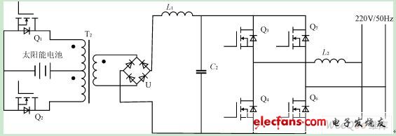
Figure 2 main circuit topology
The main circuit of the DC/AC inverter adopts a full-bridge structure, which consists of four MOS tubes (parallel antiparallel diodes inside the tube), which converts 400V DC into 220V/50Hz power frequency AC.
2.2.1 DC/DC converter control scheme
The control block diagram of the DC/DC converter is shown in Figure 3. The control circuit is based on the integrated circuit SG3525, and two 50 kHz driving signals output by the SG3525 are applied to the gates of the push-pull circuit switching tubes Q1 and Q2 via the gate driving circuit. In order to keep the output voltage of the DC/DC converter stable, the detected output voltage is compared with the command voltage, and the error voltage is controlled by the PI regulator to control the duty ratio of the SG3525 output drive signal. The control circuit also has a protection function that limits the output overcurrent and overvoltage. When it is detected that the DC/DC converter output current is too large, the SG3525 will reduce the width of the gate pulse, lower the output voltage, and thus reduce the output current. When the output voltage is too high, the operation of the DC/DC converter is stopped. Since the push-pull circuit is prone to transformer saturation due to DC bias, the design difficulty of the push-pull circuit is how to prevent the magnetic saturation of the transformer. In this circuit, in addition to paying attention to the symmetry of the circuit, a magnetic saturation detection circuit is also designed. When the currents of the two branches flowing through the push-pull circuit are unbalanced, the soft start function of the SG3525 is activated to make the DC/DC The converter is restarted and the transformer is reset.
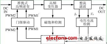
Figure 3 Control block diagram of the DC/DC converter
The bias detection circuit is shown in Figure 4. Only the secondary side of the magnetic ring is shown in the figure. The two coils on the primary side are connected to the two windings on the primary side of the transformer of the main circuit, and the current flowing through the two coils is reversed. When the transformer is biased, the current in a certain direction is abnormally large. Through the current transformer detection, a voltage can be generated on the output resistance R1 of the transformer. If the voltage is large enough, the Zener diode D5 can be turned on. A voltage drop is generated on the potentiometer, and the value of the potentiometer is adjusted to a suitable resistance value so that the voltage drop across the potentiometer is greater than the threshold voltage of the triode, so that the triode is turned on, and the capacitance between the pin 8 of the chip SG3525 and the ground is connected. Discharge, then charge the constant current source in the SG3525, and restart the SG3525 to reset the transformer core.
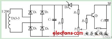
Figure 4 bias detection circuit
2.2.2 DC/AC inverter control scheme
The DC/AC inverter is the focus and difficulty of photovoltaic grid connection, so the following section will focus on this part. The DC/AC inverter control block diagram is shown in Figure 5. The core control chip uses TI's TMS320F240. Although the MCU can also realize the pulse width modulation of the grid-connected inverter, the real-time processing capability of the DSP is more powerful, so that the system can have a higher switching operating frequency. The situation of the system input and output signals can be clearly seen from Figure 5.

Figure 5 Control block diagram of the DC/AC inverter
2.3 Output power optimization control scheme
In the static case, when the grid-connected inverter is connected to the solar cell, the grid-connected inverter can be equivalent to the load resistance of the solar cell. When the light intensity λ and temperature T change, the terminal voltage of the solar cell output will change accordingly. In order to use solar energy effectively, the output of the solar cell should always be at an appropriate working point. Therefore, the control scheme requires that when the voltage of the solar cell rises, its output power can be increased; otherwise, its output power is lowered.
The control scheme of the DSP is shown in Figure 6. After the reference voltage is compared with the actual voltage of the solar cell, the error is adjusted by PI, and the obtained current command (DC amount) IREF is multiplied by the sine table value in the ROM to obtain The alternating output current command iref is compared with the actual output current value, and the error is subjected to the proportional (P) step, and the obtained command is inverted, and after the collected AC side voltage Us is added, the The resulting waveform is then compared to the triangular wave to produce four PWM modulated signals (the frequency of the triangular wave is 20 kHz).
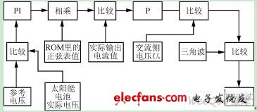
Figure 6 DSP control scheme
2.4 Detection of AC side voltage Us
By synchronizing and rectifying the synchronization signal of the secondary side of the synchronous transformer, a relatively stable direct current can be obtained and sent to the A/D conversion port of the DSP. Since the resulting DC voltage has a relatively stable relationship with the grid voltage, it is easier to convert the value of Us.
Because of the problem of common ground, the full-wave precision rectifier circuit of the operational amplifier is used, as shown in Figure 7.

Figure 7 Us rectifier circuit
2.5 Current command synchronization
When connected to the grid, the sine wave current output from the inverter is required to be the same frequency and in phase with the grid voltage. First, the grid voltage signal is filtered and shaped into a synchronous square wave signal, which is then input to the external interrupt port XINT1 of the TMS320F240 in order to capture the zero-crossing signal of the grid voltage. As shown in Figure 8, the grid voltage sine wave, after shaping, gets a square wave.
When the DSP detects the upper edge of the zero-crossing signal, it triggers the synchronous interrupt. The time point is used as the reference to give the sine wave signal time start point, that is, the sine table pointer is reset to zero; whenever the T1 underflow interrupt (PWM real-time) When controlling), the sine table pointer is incremented by one and takes values ​​from the sine table. The unit sine wave data of one cycle is divided into 400 points and stored in the memory in the form of a table. Since the sync signal is more susceptible to interference by harmonics and spike voltages, a delay can be made after entering the sync interrupt to determine whether the external interrupt pin XINT1 is still high. If it is high, the interrupt routine is executed. Otherwise, it jumps out of the interrupt routine.
It can be seen from the control scheme of Fig. 6 that after the IREF is multiplied by the data in the sine table, a current given signal of a sine wave with adjustable amplitude is formed, and then the current reference value is compared in real time, after the P link. After the obtained signal is inverted, it is added to the collected AC side grid voltage signal Us, and the obtained waveform is compared with the triangular wave, and a PWM wave is generated to control the on and off of the bridge arm. In summary, the same-frequency, in-phase requirements of the output current and the grid voltage are achieved by current tracking control.
2.6 PWM pulse width modulation wave generation
The PWM wave is generated by the TMS320F240's full comparison unit with a frequency of 20 kHz. As can be seen from Fig. 6, the modulation pulse is generated by comparing the current command value with the actual current value and then passing the P link, and the obtained waveform is compared with a triangular wave (frequency of 20 kHz). Therefore, the timing of the generation of the pulses of the MOS transistors Q3, Q4, Q5, and Q6 (see FIG. 2) can be obtained from FIG. 8, referring to the sine wave and the triangular wave modulation, and the intersection of the two determines the pulse timing of the PWM. Actually, the sampled waveform (actually a staircase wave) intersects the triangular wave, and the pulse width is obtained from the intersection. This system is a staircase wave formed by sampling a waveform at the bottom position of a triangular wave. The position of the pulse width determined by the intersection of the staircase wave and the triangular wave is symmetrical within one sampling period, as shown in FIG.
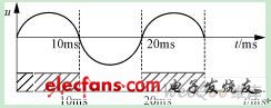
Figure 8 Synchronization signal waveform
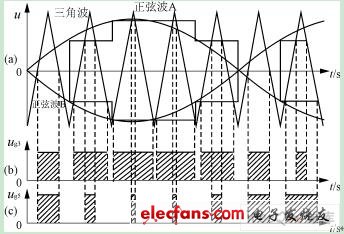
Figure 9 sinusoidal pulse width modulation waveform
Fig. 9(a) The intersection of the sine wave B and the triangular wave determines the conduction time of Q3; the intersection of the sine wave A and the triangular wave determines the conduction time of Q5.
Figure 9(b) is a schematic diagram of the pulse of Q3, the pulses of Q3 and Q4 on the same bridge arm are complementary.
Fig. 9(c) is a schematic diagram of the pulse of Q5, and the pulses of Q5 and Q6 on the same bridge arm are complementary.
2.7 TMS320F240 software control process
This part of the software is mainly divided into 4 blocks, namely the main program, T1 underflow interrupt, T2 underflow interrupt and synchronous interrupt. The flow chart is shown in Figure 10. The T1 underflow interrupt occurs every 50μs. The program is mainly used to generate PWM waves. The T2 underflow interrupt occurs every 10ms. The program is mainly used to generate current commands. The synchronous interrupt occurs approximately every 20ms (network voltage cycle).

Figure 10 software flow chart
2.8 System Protection
The system is designed with DC side overvoltage, undervoltage, AC side overcurrent, overheating and other protections. When the output voltage overvoltage or undervoltage fault of the solar panel occurs, the TMS320F240 sends a signal to the SG3525 to block the DC/DC pulse and stop it. When the DC voltage is detected to return to normal, the DC/DC is again The automatic reset starts working; when an AC overcurrent or overheat fault occurs, the program enters the interrupt service subroutine and blocks all drive signals. When the fault is removed, the system is manually reset and the system is restarted.
3 main components selection and experimental waveform
The push-pull circuit MOS transistor is IRFP350 (withstand voltage 400V, drain current rated current is 16A). The bridge inverter circuit MOS tube is selected from IRFPC40 (withstand voltage 600V, drain current rated current is 6.8A). The DC/DC filter inductor L1 selects 1.2mH, and the DC/AC filter inductor L2 selects 33.4mH.
Fig. 11 is a waveform of voltage and current when the output side of the inverter is connected to the grid. The grid side voltage is 220±20%, and the effective value of the current is about 1A.
4 Conclusion
This paper describes a control system for a low-power photovoltaic grid-connected inverter. The topology of the DC/DC controller adopts a push-pull circuit, which is controlled by the chip SG3525. This circuit effectively prevents biasing; the DC/AC inverter is a full-bridge inverter circuit, which is controlled by DSP. Because the computing speed of the DSP is relatively high, the output current of the inverter can well track the grid voltage waveform. The effectiveness of this photovoltaic grid-connected inverter control scheme was verified in the laboratory. The control system ensures that the output power factor of the inverter is close to 1, and the output current is sinusoidal.
As one of the cast resin transformer manufacturers, FGI`s Cast Resin Transformers can be used as an upgraded product of Oil Filled Distribution Transformers, which are the best performance of all kinds of dry type transformers, especially applicable to urban power grids, high-rise buildings, business centers, theaters, hospitals, hotels, tunnels, subways, underground power stations, laboratories, stations, terminals, airports, combined substations and other important places.
Cast Resin Transformers
Cast Resin Transformer,Cast Resin Dry Type Transformer,Cast Coil Transformer,Cast Resin Distribution Transformers,Cast Coil Transformers Manufacturers,Cast Resin Transformer Manufacturers
FGI SCIENCE AND TECHNOLOGY CO., LTD , https://www.fgi-tech.com