MOSFETs are widely used in switching power supplies due to their low internal resistance and fast switching speed. The drive of the MOSFET often selects the appropriate circuit based on the parameters of the power supply IC and MOSFET. Let's discuss the driving circuit of the MOSFET for the switching power supply.
When designing a switching power supply using a MOSFET, most people consider the on-resistance, maximum voltage, and maximum current of the MOSFET. But many times only these factors are considered. Such a circuit may work properly, but it is not a good design. More detailed, the MOSFET should also consider its own parasitic parameters. For a certain MOSFET, its drive circuit, the peak current of the drive pin output, the rising rate, etc., will affect the switching performance of the MOSFET.
When the power IC and MOS transistor are selected, it is especially important to select the appropriate driver circuit to connect the power IC to the MOS transistor.
A good MOSFET driver circuit has the following requirements:
(1) When the switch is turned on, the drive circuit should be able to provide a large enough charge current to quickly increase the voltage between the gate and source of the MOSFET to the desired value, ensuring that the switch can be turned on quickly and there is no high-frequency oscillation of the rising edge.
(2) The drive circuit during the on-time of the switch ensures that the voltage between the gate and source of the MOSFET remains stable and reliably turned on.
(3) The shutdown transient drive circuit can provide a path with as low impedance as possible for the rapid discharge of the capacitor voltage between the gate and source of the MOSFET, ensuring that the switch can be quickly turned off.
(4) The drive circuit structure is simple and reliable, and the loss is small.
(5) Apply isolation depending on the situation.
The MOSFET drive circuits commonly used in several module power supplies are described below.
1: The power IC directly drives the MOSFET
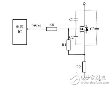
Figure 1 IC directly drives the MOSFET
The direct drive of the power IC is our most common driving method, and it is also the simplest driving method. With this driving method, we should pay attention to several parameters and the influence of these parameters. First, look at the power IC manual, which has a maximum drive peak current. Because of different chips, the drive capability is often different. Second, look at the parasitic capacitance of the MOSFET, as shown in Figure 1, the values ​​of C1 and C2. If the values ​​of C1 and C2 are relatively large, the energy required to turn on the MOS transistor is relatively large. If the power IC does not have a large driving peak current, the conduction speed of the tube is relatively slow. If the driving ability is insufficient, high-frequency oscillation may occur on the rising edge. Even if the Rg in Fig. 1 is reduced, the problem cannot be solved! Factors such as IC drive capability, MOS parasitic capacitance, and MOS tube switching speed all affect the selection of the resistance of the drive resistor, so Rg cannot be reduced indefinitely.
2: When the power IC drive capability is insufficient
If the parasitic capacitance of the MOS transistor is relatively large, and the driving capability inside the power IC is insufficient, the driving capability needs to be enhanced on the driving circuit, and the totem pole circuit is often used to increase the driving capability of the power IC. The circuit is shown in the dotted line of FIG.

Figure 2 Totem pole drive MOS
The function of this driving circuit is to improve the current supply capability and quickly complete the charging process for the gate input capacitor charge. This topology increases the time required for conduction, but reduces the turn-off time, the switch can be turned on quickly and avoids high frequency oscillations at the rising edge.
3: Drive circuit accelerates MOS tube turn-off time

Figure 3 Accelerating MOS shutdown
The shutdown instant drive circuit can provide a path with as low impedance as possible to quickly discharge the capacitor voltage between the gate and source of the MOSFET, ensuring that the switch can be quickly turned off. In order to quickly discharge the capacitance between the gate and the source, a resistor and a diode are often connected in parallel with the driving resistor, as shown in Fig. 3. Among them, D1 is commonly used as a fast recovery diode. This reduces the turn-off time while reducing the losses at turn-off. Rg2 is to prevent the current from being too large when the shutdown is turned off, and the power IC is burned off.
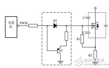
Figure 4 Improved Acceleration MOS Shutdown
The totem pole circuit introduced at the second point also has an accelerated turn-off effect. When the driving capability of the power IC is sufficient, the circuit improvement in FIG. 2 can accelerate the turn-off time of the MOS transistor, and the circuit shown in FIG. 4 is obtained. It is quite common to use a triode to bleed the gate-to-source capacitance voltage. If the emitter of Q1 has no resistance, when the PNP transistor is turned on, the capacitance between the gate and source is shorted, and the charge is discharged in the shortest time to minimize the crossover loss at the time of turn-off. Compared with the topology of Figure 3, there is also the advantage that the current on the capacitance between the gate and source is not discharged through the power IC, which improves the reliability.
4: Drive circuit accelerates MOS tube turn-off time
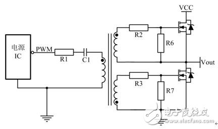
Figure 5 isolated drive
In order to satisfy the driving of the high-end MOS tube as shown in Fig. 5, a transformer drive is often used, and sometimes a transformer drive is used to satisfy the safety isolation. The purpose of R1 is to suppress the parasitic inductance on the PCB and form LC oscillation with C1. The purpose of C1 is to separate DC, through AC, and also prevent core saturation.
In addition to the above drive circuits, there are many other forms of drive circuits. It is best to have no driver circuit for a wide variety of driver circuits. Only the most suitable driver can be selected in combination with the specific application.
Instrumentation Cable Assembly
Kable-X focuses on the development and production of high-quality custom wiring harness. Terminals are indispensable parts in the processing of cable assembly. There are also many types of terminals, including disc terminals, tube terminals, Y-shaped terminals, 250 terminals, etc. Etc., as the market continues to grow and customers' quality requirements continue to increase, Kable-X' s requirements for purchasing terminals are also very strict. All terminal incoming materials must meet the requirements described in the corresponding specifications.
In addition to Instrumentation Cable Assembly, we also have Vehicle Cable Assembly and Industrial Cable Assembly.

Instrumentation Cable Assembly,Instrument Wiring Harness,Instrument Cable Assembly,Instrument Wiring Harnesses
Kable-X Technology (Suzhou) Co., Ltd , https://www.kable-x-tech.com