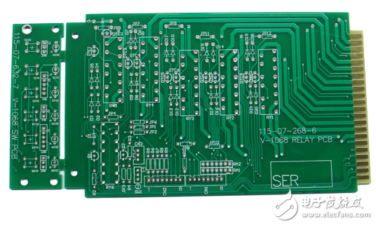
The first step is to obtain a PCB. Begin by carefully documenting the model, specifications, and placement of all components on paper. Pay special attention to the orientation of diodes, transistors, and the notch position on ICs. It’s highly recommended to take high-resolution photos of both sides of the board using a digital camera for reference later.

Next, remove all components from the PCB and desolder any excess solder from the pads. Clean the board thoroughly with isopropyl alcohol to ensure a clear surface. Place the cleaned PCB in a flatbed scanner, launch Photoshop, and scan the silkscreen side in color. Print this image for future use as a reference guide.
In the third step, gently sand the top and bottom layers of the PCB using fine-grit wet/dry sandpaper until the copper traces are visible. Make sure to keep the board flat and clean during this process. Then, place it back into the scanner, open Photoshop, and scan each layer separately in color. Be careful to keep the PCB perfectly horizontal, or the scanned images may not align properly.
The fourth step involves adjusting the contrast and brightness of the scanned images so that the copper areas stand out clearly against the non-copper regions. Convert the images to black and white and check if the lines are sharp and well-defined. If the image isn’t clear, repeat the adjustment process. Once satisfied, save the final images as black and white BMP files named TOP.BMP and BOT.BMP.
Now, convert the two BMP files into PROTEL-compatible format and import them into PROTEL as separate layers. Check if the PAD and VIA positions on both layers align correctly. A good alignment indicates that the previous steps were done accurately. If there's a mismatch, go back and re-scan the layers.
Proceed by converting the TOP.BMP file into a TOP.PCB file in PROTEL. Be sure to assign it to the SILK (yellow) layer. Then, trace the top layer lines and place the components according to the layout you created in step two. After completing the tracing, remove the SILK layer from the top design.
Repeat the same process for the BOT.BMP file, converting it into a BOT.PCB file and assigning it to the SILK layer. Trace the bottom layer lines and place the components accordingly. Once done, delete the SILK layer from the bottom design.
Finally, combine the TOP.PCB and BOT.PCB layers into a single image. This will serve as your final layout for further processing or manufacturing.
As a final verification step, print the TOP LAYER and BOTTOM LAYER onto transparent film at a 1:1 scale using a laser printer. Place the film over the original PCB and compare it for any discrepancies. If everything matches up, you're all set and ready for the next stage of your project.
3D Metal Letter,Custom Metal Channel Letters,Outdoor 3D Metal Signage,Metal Channel Letters
Wuxi Motian Signage Co., Ltd , https://www.makesignage.com