The first step is to obtain a PCB. Begin by carefully documenting the model, specifications, and placement of all components on paper. Pay special attention to the orientation of diodes, transistors, and the notch direction on ICs. It's highly recommended to take photos of both sides of the board using a digital camera for reference. 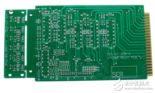
In the second step, carefully remove all components from the PCB and desolder any excess tin from the PAD holes. Clean the board thoroughly with isopropyl alcohol. Then place it in a scanner and use Photoshop to scan the silk screen layer in color. Print this out for future reference during the tracing process.
For the third step, gently polish the TOP LAYER and BOTTOM LAYER using fine-grit sandpaper to expose the copper surface. Place the board flat in the scanner again, launch Photoshop, and scan each layer separately in color. Make sure the PCB is perfectly horizontal in the scanner—any tilt can cause misalignment in the final image.
The fourth step involves adjusting the contrast and brightness in Photoshop so that the copper areas stand out clearly against the non-copper parts. Convert the images to black and white and check if the lines are sharp and clear. If not, repeat the adjustment until the image is clean. Save the final images as black and white BMP files named TOP.BMP and BOT.BMP.
In the fifth step, convert the two BMP files into PROTEL format and import them into the respective layers in PROTEL. If the PAD and VIA positions align correctly between the two layers, it means the previous steps were done accurately. If there’s a mismatch, go back and re-scan the layers.
The sixth step is to convert the TOP.BMP file into a TOP.PCB layer. Be careful to assign it to the SILK layer (the yellow layer). Then, trace the circuit lines on the TOP layer and place the components according to your original notes. After completing the layout, remove the SILK layer.
The seventh step follows a similar process for the BOT.BMP file. Convert it to BOT.PCB, assign it to the SILK layer, and trace the bottom layer lines. Once finished, remove the SILK layer again.
The eighth step involves merging the TOP.PCB and BOT.PCB layers into a single image for verification. This helps ensure that the design is accurate before moving forward.
In the ninth step, print the TOP LAYER and BOTTOM LAYER on transparent film using a laser printer at a 1:1 scale. Place the film over the PCB and compare it with the actual board to check for any discrepancies. If everything matches, you’re done! This method is commonly used for creating custom PCB layouts from existing boards.
Aluminium Led Channel Letter,Led Aluminum Channel Signs,Custom Channel Letter Signs,Led Backlit Aluminum Channel Letters
Wuxi Motian Signage Co., Ltd , https://www.makesignage.com