1. Forward voltage is reduced, dark light 
A: One is that the electrode is in ohmic contact with the luminescent material, but the contact resistance is large, mainly due to the low concentration of the material substrate or the defect of the electrode.
B: One is that the electrode and the material are non-ohmic contact, mainly occurs in the extrusion printing or the printing position when the first layer electrode is evaporated during the preparation of the chip electrode, and the distribution position.
In addition, the forward pressure may also be reduced during the packaging process. The main reason is that the silver gel is not sufficiently cured, and the contact or chip electrode is contaminated, resulting in large contact resistance or unstable contact resistance.
When the chip with reduced forward voltage is tested at a fixed voltage, the current passing through the chip is small, thereby expressing a dark spot. Another dark light phenomenon is that the chip itself has low luminous efficiency and a normal forward voltage drop.
2. Difficult pressure welding: (mainly non-stick, electrode peeling, piercing the electrode)
A: It is not sticky: mainly because the surface of the electrode is oxidized or has glue
B: There is a weak contact with the luminescent material and the thickened bonding wire layer is not strong, and the thick layer is mainly detached.
C: Breaking the electrode: usually related to the chip material, the material is brittle and the strength is not high, the material is easy to penetrate the electrode. Generally, the GAALAS material (such as high red, infrared chip) is easier to penetrate the electrode than the GAP material.
D: Pressure welding adjustment should be adjusted from welding temperature, ultrasonic power, ultrasonic time, pressure, gold ball size, bracket positioning and so on.
3. Difference in illuminating color:
A: The difference in the color of the same chip is mainly due to the problem of the epitaxial wafer material. The ALGAINP four-element material is very thin in quantum structure, and it is difficult to ensure the uniformity of the composition in each region. (The component determines the forbidden band width and the forbidden band width determines the wavelength).
B: GAP yellow-green chip, the wavelength of light will not be greatly deviated, but because the human eye is sensitive to the color of this band, it is easy to detect yellowish and greenish. Since the wavelength is determined by the material of the epitaxial wafer, the smaller the region, the smaller the concept of color deviation, so there is a proximity selection method in the M/T operation.
C: The GAP red chip has a luminescent color that is orange-yellow, because its luminescence mechanism is an indirect leap. Affected by the impurity concentration, when the current density is increased, impurity level shift and luminescence saturation are likely to occur, and the luminescence starts to turn orange.
4. The thyristor effect;
A: The LED cannot be turned on under normal voltage. When the voltage is raised to a certain level, the current is abrupt.
B: The cause of the thyristant phenomenon is that the reverse interlayer occurs when the epitaxial wafer of the luminescent material grows. The forward voltage drop of the LED with this phenomenon is hidden at IF=20MA, and the process is due to the fact that the voltage of the two poles is not large enough. The performance is not bright. The test information instrument can be used to test the curve from the transistor plotter. It can also be found by the forward voltage drop at a small current of IF=10 UA. The forward voltage drop at a small current is obviously too large, which may be This problem is caused by.
5. Reverse leakage:
A: Reason: Epitaxial material, chip fabrication, device package, test, the general leakage current is 5UA under 5V, and the reverse voltage can be tested under fixed reverse current.
B: The reverse characteristics of different types of LEDs are quite different: the green color, the reverse breakdown of the yellow chip can reach more than one hundred volts, and the chip is between ten and twenty volts.
C: The reverse leakage caused by epitaxy is mainly caused by the internal structural defects of the PN junction. The side corrosion is not enough or the silver rubber wire is attached to the measuring surface during the chip making process. It is strictly forbidden to use the organic solution to prepare the silver paste. In order to prevent the silver glue from climbing to the knot area through capillary phenomenon.
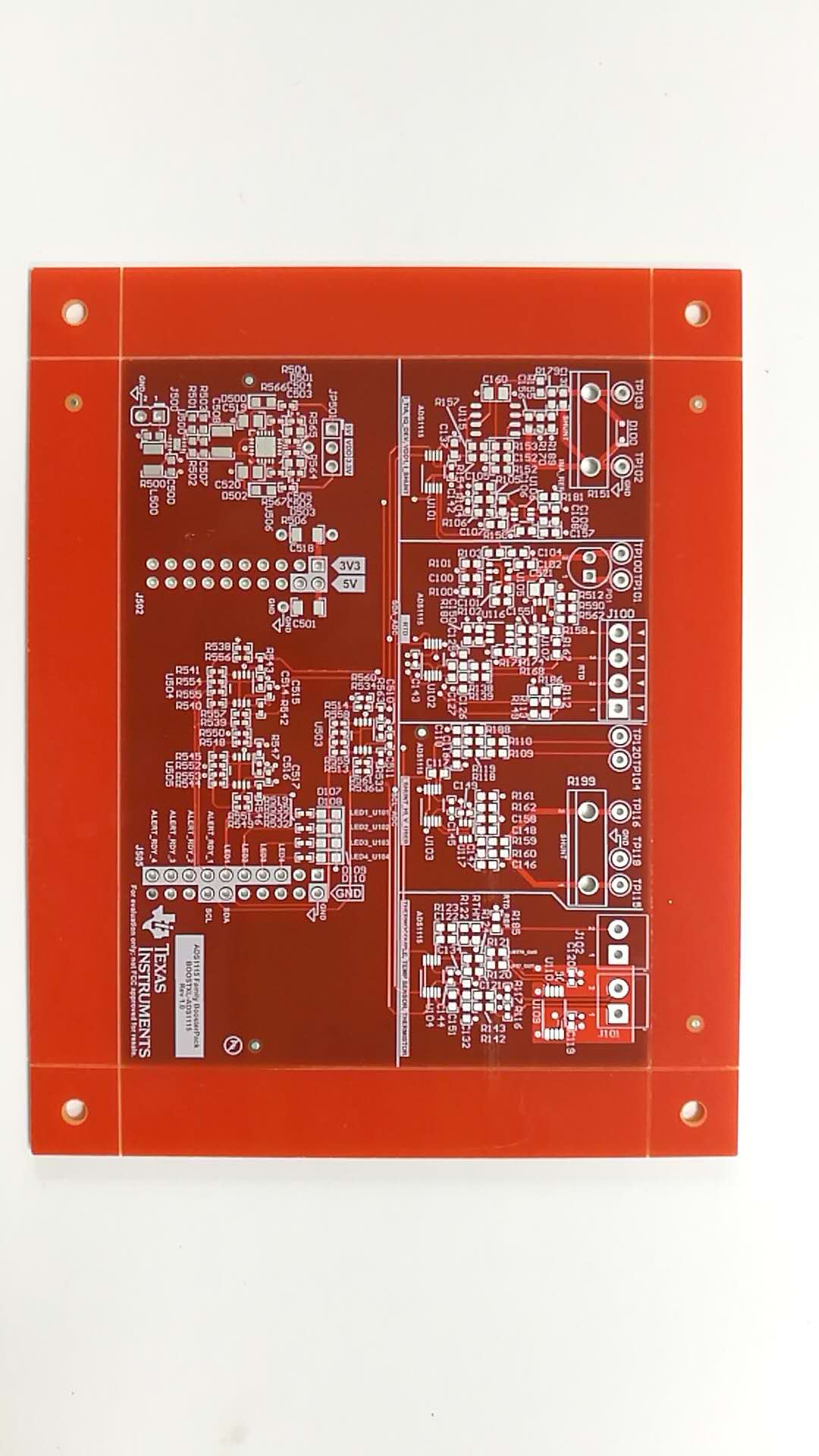
Printed Circuit Board (PCB) mechanically supports and electrically connects Electronic Components or electrical components using conductive tracks, pads and other features etched from one or more sheet layers of copper laminated onto and/or between sheet layers of a non-conductive substrate. Components are generally soldered onto the PCB to both electrically connect and mechanically fasten them to it.
Printed circuit boards are used in all but the simplest Electronic Products. They are also used in all kinds of electrical products

Printed Circuit Board
Printed Circuit Board,Multilayer Printing Circuit Board,Motherboard Printed Circuit Board,Professional Printed Circuit Board
Orilind Limited Company , https://www.orilind.com